 ChipApex | Global Electronic Components Supplier
SEARCH
Search Product
Search Post
— IC芯片 | 连接器 | 传感器 | 被动器件 —
Search productSearch post
— IC芯片 | 连接器 | 传感器 | 被动器件 —
Consult the customer manager about the wholesale price.
consultation hotline:86-132-6715-2157
email:[email protected]
Contact the product manager for consultation. One-stop consultation is available.
Do you want a lower wholesale price? Please send us your inquiry and we will reply immediately.
The A54SX16A-1FGG256M is a Field Programmable Gate Array from the SX-A family, manufactured by Microchip Technology. It features 24,000 system gates and supports up to 180 user-programmable I/O pins within a 256-pin Fine Pitch Ball Grid Array (FBGA) package. The device operates at a maximum frequency of 263 MHz with a supply voltage range of 2.25 V to 2.75 V. It utilizes 0.22 μm / 0.25 μm CMOS antifuse technology and supports an operating temperature range from -55°C to +125°C.
Verify component authenticity through authorized Microchip distributors or direct manufacturer channels. Confirm that the specific ordering suffix matches the required speed grade, package type, and temperature range. Ensure proper handling procedures are followed due to moisture sensitivity classification. Review current availability status as production lifecycles may affect supply continuity.
Select this model when 24,000 system gates and 180 I/Os are required in a 256-pin FBGA form factor. Ensure the design accommodates the 2.25 V to 2.75 V supply voltage range. Verify that the -1 speed grade meets the target 263 MHz performance requirements. Consider the military temperature grade (-55°C to +125°C) if environmental conditions necessitate extended operational ranges.
This component belongs to the Actel SX-A family of FPGAs, which were originally developed by Actel Corporation before being acquired by Microsemi and subsequently Microchip Technology. The SX-A series is characterized by its antifuse-based architecture, offering high performance and security against reverse engineering. This specific part represents a mid-range capacity device within the family, balancing gate count with pin density.
Direct replacements within the same package and pinout include other speed grades of the A54SX16A series, such as the standard speed variant or faster grades like -2, provided timing constraints allow. Cross-family migration to newer Microchip FPGA architectures requires significant redesign due to architectural differences between antifuse and SRAM-based technologies.
The device uses metal-to-metal programmable antifuse technology fabricated on a 0.22 μm / 0.25 μm CMOS process, providing nonvolatile configuration.
Yes, the SX-A family supports power-up/down friendly operation where VCCA and VCCI do not need to be stable during power transitions and can be powered in any order.
Yes, all SX-A devices support Boundary-Scan Testing (BST) in compliance with IEEE Standard 1149.1 (JTAG).
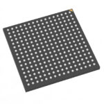 A54SX16A-1FGG256M
The activity of extra discounts on wholesale prices is in full swing…
Please fill in your contact information and we will send you the latest wholesale price list.





