 ChipApex | Global Electronic Components Supplier
SEARCH
Search Product
Search Post
— IC芯片 | 连接器 | 传感器 | 被动器件 —
Search productSearch post
— IC芯片 | 连接器 | 传感器 | 被动器件 —
Consult the customer manager about the wholesale price.
consultation hotline:86-132-6715-2157
email:[email protected]
Contact the product manager for consultation. One-stop consultation is available.
Do you want a lower wholesale price? Please send us your inquiry and we will reply immediately.
The A54SX32-PQG208I is a Field Programmable Gate Array from the Microchip SX-A family, featuring 48,000 system gates and 174 user-programmable I/Os. It utilizes 0.22 μm / 0.25 μm CMOS antifuse technology to achieve up to 350 MHz internal performance with a 250 MHz system clock speed. The device operates at 2.5 V, 3.3 V, or 5.0 V with mixed-voltage support and includes 1,080 dedicated flip-flops. It is housed in a 208-pin Plastic Quad Flat Pack (PQFP) package and supports an industrial temperature range of -40°C to +85°C.
Verify the specific ordering suffix against the manufacturer's current datasheet to confirm package type and temperature grade. Confirm RoHS compliance status as standard packaging may differ from lead-free options. Check for any product discontinuation notices or lifecycle changes before finalizing procurement plans.
Select this model when 48,000 system gates and 208-pin PQFP packaging are required. Ensure the design benefits from nonvolatile antifuse technology and mixed-voltage I/O flexibility. Verify that the industrial temperature range meets environmental specifications.
This component belongs to the Actel SX-A FPGA family, which uses metal-to-metal programmable antifuse interconnect elements. The architecture features a sea-of-modules design with register cells and combinatorial cells arranged in clusters for optimal resource utilization.
Consult the official datasheet for alternative packages within the A54SX32A series, such as FBGA variants. Verify pin compatibility and electrical characteristics when considering cross-package replacements.
The device supports internal clock frequencies up to 350 MHz.
Yes, it supports 2.5 V, 3.3 V, and 5.0 V mixed-voltage operation with 5.0 V input tolerance.
The A54SX32A provides two routed global clocks (CLKA, CLKB) and one hardwired clock (HCLK).


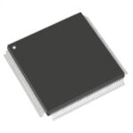 A54SX32-PQG208I
The activity of extra discounts on wholesale prices is in full swing…
Please fill in your contact information and we will send you the latest wholesale price list.



