 ChipApex | Global Electronic Components Supplier
SEARCH
Search Product
Search Post
— IC芯片 | 连接器 | 传感器 | 被动器件 —
Search productSearch post
— IC芯片 | 连接器 | 传感器 | 被动器件 —
Consult the customer manager about the wholesale price.
consultation hotline:86-132-6715-2157
email:[email protected]
Contact the product manager for consultation. One-stop consultation is available.
Do you want a lower wholesale price? Please send us your inquiry and we will reply immediately.
The A54SX32A-2TQG100 is a Field Programmable Gate Array from the SX-A family, featuring 48,000 system gates and 81 user-programmable I/Os. It utilizes 0.22 μm / 0.25 μm CMOS antifuse technology to provide deterministic timing with up to 100% resource utilization and pin locking. The device supports mixed-voltage operation at 2.5 V, 3.3 V, and 5 V with 5 V input tolerance. It operates within an industrial temperature range of -40°C to +85°C and is housed in a 100-pin Thin Quad Flat Pack (TQFP) package.
Verify the specific ordering suffix 'I' confirms the industrial temperature grade (-40°C to +85°C). Confirm the '2' speed grade indicates approximately 25% faster performance than standard. Ensure the TQFP package type matches the design footprint. Check for RoHS compliance status if required by assembly specifications.
Select this model for applications requiring 48K system gates with industrial temperature stability. The -2 speed grade offers higher frequency performance compared to standard grades. Verify that the 100-pin TQFP package fits the PCB constraints. Consider the 5V tolerant I/Os if interfacing with legacy components.
This component belongs to the Microchip (formerly Actel) SX-A FPGA family, which uses nonvolatile antifuse technology. The A54SX32A variant provides 48,000 system gates, positioning it between the smaller A54SX16A and larger A54SX72A devices in terms of capacity and I/O availability.
Public confirmed substitute part numbers are not available in the provided documentation.
The SX-A family supports internal clock frequencies up to 350 MHz.
DirectConnect provides a hardwired signal path between a C-cell and its neighboring R-cell within a SuperCluster, achieving a maximum routing delay of less than 0.1 ns without using programmable antifuses.
Yes, in Flexible mode, TDI, TCK, and TDO may function as user I/Os or BST pins, while TMS cannot be employed as a user I/O in either mode.
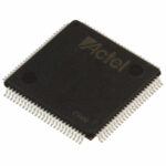 A54SX32A-2TQG100
The activity of extra discounts on wholesale prices is in full swing…
Please fill in your contact information and we will send you the latest wholesale price list.





