ChipApex | Global Electronic Components Supplier
SEARCH
Search Product
Search Post
— IC芯片 | 连接器 | 传感器 | 被动器件 —
Search productSearch post
— IC芯片 | 连接器 | 传感器 | 被动器件 —
Consult the customer manager about the wholesale price.
consultation hotline:86-132-6715-2157
email:[email protected]
Contact the product manager for consultation. One-stop consultation is available.
Do you want a lower wholesale price? Please send us your inquiry and we will reply immediately.
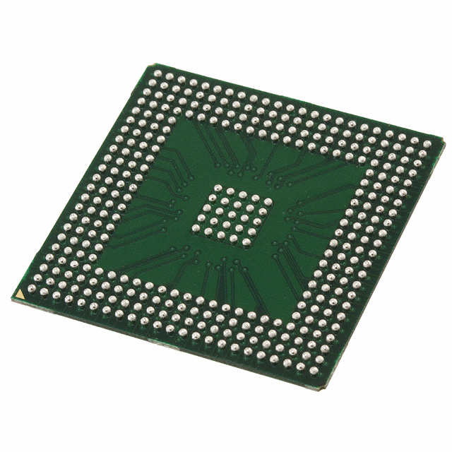
The A54SX32A-BGG329I is a Field Programmable Gate Array from the Microchip Actel SX-A family, featuring 48,000 system gates and 2,880 logic modules. It supports up to 249 user-programmable I/O pins and utilizes 0.22 μm / 0.25 μm CMOS antifuse technology. The device operates at a maximum internal frequency of 350 MHz with a system performance of 250 MHz. It accommodates mixed-voltage operation at 2.5 V, 3.3 V, and 5 V with 5 V input tolerance. The component is housed in a 329-pin Plastic Ball Grid Array (PBGA) package and is rated for industrial temperature ranges (-40°C to +85°C).
Verify the specific speed grade suffix associated with this part number against official Microchip documentation to ensure correct timing characteristics. Confirm RoHS compliance status as packaging options vary. Check for any Product Change Notifications regarding manufacturing updates or obsolescence notices before finalizing procurement plans.
Select this model when 48,000 system gates and 249 I/Os are required within a 329-pin BGA footprint. Ensure the design leverages the 2.5 V, 3.3 V, and 5 V mixed-voltage capabilities if interfacing with diverse logic families. Verify that the industrial temperature range meets the environmental requirements of the target application.
This component belongs to the Actel SX-A family of FPGAs, which are built on high-voltage twin-well CMOS process technology. The family includes devices ranging from 12,000 to 108,000 system gates, offering various package options and speed grades to suit different performance and pin-count needs.
Direct replacements within the same package and pinout include other speed grades of the A54SX32A series such as A54SX32A-FBGG329 or A54SX32A-TQG100A, provided the timing specifications meet the design requirements. Cross-family migration to newer Microchip FPGA architectures requires schematic and code re-verification.
The device features three clock networks: one hardwired HCLK buffer and two routed global clocks (CLKA, CLKB), ensuring fast and predictable signal propagation across the chip.
The device uses Actel Secure Programming Technology with FuseLock™, which prevents reverse engineering by making it difficult to distinguish programmed antifuses and blocks unauthorized reading of the configuration.
No, unused I/O pins must be configured as tristate outputs or tied to a defined logic level (High or Low) to prevent undefined states and potential current leakage.
 A54SX32A-BGG329I
The activity of extra discounts on wholesale prices is in full swing…
Please fill in your contact information and we will send you the latest wholesale price list.