 ChipApex | Global Electronic Components Supplier
SEARCH
Search Product
Search Post
— IC芯片 | 连接器 | 传感器 | 被动器件 —
Search productSearch post
— IC芯片 | 连接器 | 传感器 | 被动器件 —
Consult the customer manager about the wholesale price.
consultation hotline:86-132-6715-2157
email:[email protected]
Contact the product manager for consultation. One-stop consultation is available.
Do you want a lower wholesale price? Please send us your inquiry and we will reply immediately.
The A54SX72A-1PQ208I is an industrial-grade FPGA from the SX-A family, utilizing 0.22 μm / 0.25 μm CMOS antifuse technology. It provides 108,000 system gates and supports up to 360 user-programmable I/O pins. The device features 6,036 logic modules (CLBs), 4,024 combinatorial cells, and 2,012 dedicated flip-flops. It operates within a voltage range of 2.25V to 5.25V and functions at temperatures between -40°C and +85°C. Packaged in a 208-pin Plastic Quad Flat Pack (PQFP), it includes three global clocks and four quadrant clocks for optimized timing.
Verify component authenticity by checking markings against official Microchip documentation. Confirm the specific ordering suffix matches the required speed grade and temperature rating. Ensure the package type aligns with PCB footprint requirements. Review datasheet specifications for electrical characteristics before finalizing procurement decisions.
Select this model when high gate density and robust security features are required. The industrial temperature range suits harsh environments. Verify that the PQFP package fits the available board space. Consider the specific speed grade requirements relative to system clock frequencies. Evaluate the I/O count against interface needs.
This component belongs to the SX-A family of FPGAs manufactured by Microchip Technology. The family utilizes antifuse technology for permanent configuration. The A54SX72A represents the highest capacity device in this series, offering maximum logic resources and I/O flexibility compared to smaller variants like the A54SX08A or A54SX32A.
Direct replacements within the same package and pinout include other speed grades of the A54SX72A, such as the standard speed version or faster variants if timing permits. Cross-family migration requires careful review of architecture differences and pin compatibility.
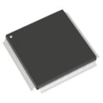 A54SX72A-1PQ208I
The activity of extra discounts on wholesale prices is in full swing…
Please fill in your contact information and we will send you the latest wholesale price list.






