 ChipApex | Global Electronic Components Supplier
SEARCH
Search Product
Search Post
— IC芯片 | 连接器 | 传感器 | 被动器件 —
Search productSearch post
— IC芯片 | 连接器 | 传感器 | 被动器件 —
Consult the customer manager about the wholesale price.
consultation hotline:86-132-6715-2157
email:[email protected]
Contact the product manager for consultation. One-stop consultation is available.
Do you want a lower wholesale price? Please send us your inquiry and we will reply immediately.
The AD808-622BR is a fiber optic receiver with quantizer, clock recovery, and data retiming for 622 Mbps NRZ data. It meets CCITT G.958 STM-4 Type A and Bellcore OC-12 requirements. Key electrical parameters include a nominal center frequency of 622.08 MHz, capture range of 620–624 MHz, and tracking range of 620–624 MHz. Output jitter is typically 2.5 degrees RMS. The device operates from a single +5 V or –5.2 V supply, consuming 400 mW. Quantizer sensitivity is 4 mV typical, with an input resistance of 10 kΩ and capacitance of 2 pF.
Verify that the component matches the specific AD808-622BR variant, as Rochester Electronics distributes recovered parts. Confirm the package is the 16-lead narrow SOIC (R-16A) and check the temperature range rating of -40°C to +85°C. Ensure the ordering suffix corresponds to the desired reel or tube configuration if applicable, though standard retail units are typically in tubes. Cross-reference the manufacturer's lot code against current quality assurance standards.
Select this component when designing SONET OC-12 or SDH STM-4 compliant optical links requiring integrated clock recovery. It is suitable for applications needing low jitter performance without external timing components. Consider the single-supply operation and low power consumption for portable or dense telecom equipment. Ensure the design accommodates the required damping capacitor for loop stability and the programmable threshold resistor for signal detection.
The AD808 is part of Analog Devices' high-speed fiber optic receiver portfolio. It combines analog quantization with digital retiming functions. The BR suffix indicates the 16-lead narrow SOIC package option. This device simplifies system design by integrating the PLL and quantizer into a single monolithic circuit, reducing board space compared to discrete solutions.
Publicly confirmed substitutes are not available in the provided documentation. Verify compatibility with existing PCB footprints and pin assignments if considering alternative manufacturers. Check if other AD808 variants meet the specific frequency and packaging requirements.
No, the AD808 uses a factory-trimmed VCO and a frequency acquisition control loop that allows it to acquire lock on random or scrambled data without a preamble or external crystal.
Jitter peaking is controlled by the damping factor capacitor (CD) connected between pins CF1 and CF2. Using a 0.47 μF capacitor provides less than 0.1 dB of jitter peaking.
The SDOUT pin provides a signal detect output that indicates whether the input signal amplitude is above or below a user-adjustable threshold, helping to manage loss of signal conditions.
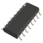 AD808-622BR
The activity of extra discounts on wholesale prices is in full swing…
Please fill in your contact information and we will send you the latest wholesale price list.





