 ChipApex | Global Electronic Components Supplier
SEARCH
Search Product
Search Post
— IC芯片 | 连接器 | 传感器 | 被动器件 —
Search productSearch post
— IC芯片 | 连接器 | 传感器 | 被动器件 —
Consult the customer manager about the wholesale price.
consultation hotline:86-132-6715-2157
email:[email protected]
Contact the product manager for consultation. One-stop consultation is available.
Do you want a lower wholesale price? Please send us your inquiry and we will reply immediately.
The AD8113JSTZ is a fully buffered analog and digital crosspoint switch matrix featuring a 16x16 nonblocking array with a fixed gain of +2. It operates on dual supplies of ±5 V for video applications or ±12 V for audio applications, consuming 34 mA or 31 mA respectively. The device provides a –3 dB signal bandwidth exceeding 60 MHz and channel switch times under 60 ns. Key performance metrics include –83 dB crosstalk at 20 kHz, 90 dB isolation, and 0.002% total harmonic distortion at 20 kHz with ±12 V supplies. It is housed in a 100-lead LQFP package and supports serial or parallel programming interfaces.
Verify the component authenticity by checking the marking code against Analog Devices documentation. Confirm the suffix JSTZ corresponds to the commercial temperature range (0°C to 70°C) and the 100-lead LQFP package. Ensure the device is handled with appropriate ESD precautions due to its sensitivity. Cross-reference the specific revision level if critical timing parameters are required for the design.
Select this component for applications requiring a fully buffered 16x16 crosspoint matrix with low distortion. Choose ±12 V supplies for audio routing to achieve higher output swing and lower THD. Use ±5 V supplies for video applications to drive 150 Ω loads efficiently. Consider the power dissipation limits when operating at higher ambient temperatures or driving heavy loads. Verify interface compatibility with either serial or parallel control logic.
The AD8113JSTZ belongs to the AD8113 series of analog and digital crosspoint switches manufactured by Analog Devices. It is part of a family designed for high-performance audio and video signal routing. The device integrates 256 transconductance stages arranged in a 16x16 matrix, providing a complete solution for signal switching with minimal external components.
The AD8113ASTZ is a related variant within the same product family, offering different performance characteristics such as higher bandwidth. Verify pinout compatibility and electrical specifications before substitution. No direct public substitute part numbers are confirmed for this specific model.
The valid input voltage range is ±5 V when operated with ±12 V supplies and ±1.5 V when operated with ±5 V supplies.
It uses a unique bias current compensation scheme that samples and cancels contributions from each transconductance stage, resulting in a residual bias current of nominally zero regardless of the number of enabled inputs.
Yes, unused outputs can be disabled to minimize loading, and the serial data out pin allows daisy-chaining multiple devices for single-pin programming of larger switch arrays.
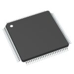 AD8113JSTZ
The activity of extra discounts on wholesale prices is in full swing…
Please fill in your contact information and we will send you the latest wholesale price list.





