 ChipApex | Global Electronic Components Supplier
SEARCH
Search Product
Search Post
— IC芯片 | 连接器 | 传感器 | 被动器件 —
Search productSearch post
— IC芯片 | 连接器 | 传感器 | 被动器件 —
Consult the customer manager about the wholesale price.
consultation hotline:86-132-6715-2157
email:[email protected]
Contact the product manager for consultation. One-stop consultation is available.
Do you want a lower wholesale price? Please send us your inquiry and we will reply immediately.
The AD8324JRQZ is a single-channel, low-cost cable line driver designed for 3.3 V upstream coaxial applications. It operates from a supply voltage range of 3.13 V to 3.47 V with a typical quiescent current of 207 mA at maximum gain. The device provides a digitally programmable voltage gain range of 59 dB with 1 dB/LSB resolution via an SPI interface. It features a 100 MHz upper bandwidth and maintains a differential output impedance of 75 Ω in both transmit-enable and transmit-disable states.
Verify the specific package variant when ordering, as the AD8324 series includes both LFCSP and QSOP options. Confirm that the JRQZ suffix corresponds to the 20-lead QSOP package required for your PCB layout. Ensure compatibility with existing SPI control logic, noting that the two most significant bits of an 8-bit word are ignored by the device. Check for moisture sensitivity levels if using surface-mount assembly processes.
Select this component for upstream cable driver applications requiring precise digital gain control. The device supports both single-ended and differential input configurations, offering flexibility in front-end design. Consider the thermal resistance characteristics of the QSOP package for heat dissipation planning. Verify that the system timing requirements for CLK, SDATA, and DATEN signals align with the specified setup and hold times.
The AD8324 is part of Analog Devices' specialized amplifier portfolio focused on cable infrastructure. It serves as a key component in hybrid fiber-coaxial (HFC) network upgrades, enabling efficient upstream data transmission. The device integrates attenuation cores and output stages optimized for low distortion and high linearity in broadband communication environments.
Public documentation confirms the AD8324ACPZ as a functional equivalent within the same family, differing primarily in the LFCSP package format. When substituting, ensure the pinout compatibility between the QSOP and LFCSP packages is addressed through appropriate PCB footprint adjustments or adapter solutions.
The device maintains a differential output impedance of 75 ± 30% Ω in both transmit-enable and transmit-disable conditions, eliminating the need for external back-termination resistors.
Asserting Logic 0 on the SLEEP pin reduces the supply current to approximately 30 µA, providing a deep power-down state beyond the standard transmit disable mode.
Yes, the AD8324 accepts either differential or single-ended input signals. For single-ended operation, the input resistance is specified at 550 Ω.
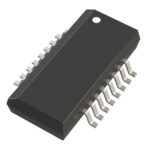 AD8324JRQZ
The activity of extra discounts on wholesale prices is in full swing…
Please fill in your contact information and we will send you the latest wholesale price list.





