 ChipApex | Global Electronic Components Supplier
AD9524BCPZ-REEL7
Search Product
Search Post
— IC芯片 | 连接器 | 传感器 | 被动器件 —
Search productSearch post
— IC芯片 | 连接器 | 传感器 | 被动器件 —
Consult the customer manager about the wholesale price.
consultation hotline:86-132-6715-2157
email:[email protected]
Contact the product manager for consultation. One-stop consultation is available.
Do you want a lower wholesale price? Please send us your inquiry and we will reply immediately.
The AD9524BCPZ-REEL7 is a jitter cleaner and clock generator featuring a dual PLL architecture with an integrated VCO tuning from 3.6 GHz to 4.0 GHz. It provides six differential or thirteen LVCMOS outputs, supporting frequencies up to 1 GHz. The device achieves absolute output jitter below 200 fs at 122.88 MHz (12 kHz to 20 MHz integration). Key specifications include input-to-output edge timing under ±150 ps, output-to-output skew under ±50 ps, and 63-step adjustable delay resolution. It operates on 3.3 V supplies for PLLs and drivers, with a 1.8 V supply for dividers, within a -40°C to +85°C temperature range.
Verify the REEL7 suffix indicates tape-and-reel packaging rather than tray packaging when sourcing. Confirm the specific grade and revision against the manufacturer's current ordering guide, as package dimensions and thermal characteristics are defined by the 48-LFCSP-VQ form factor.
Select this component for applications requiring sub-picosecond jitter performance and flexible output formatting. Ensure the design accommodates the required 3.3 V and 1.8 V supply rails. Verify that the external VCXO reference meets the accuracy requirements for the specified startup frequency tolerance of ±100 ppm.
The AD9524 belongs to Analog Devices' family of high-performance clock generators designed for demanding telecommunications and data converter synchronization tasks. It serves as a critical timing element in systems where phase noise and jitter directly impact signal integrity and system throughput.
Cross-reference with other ADI clock generators such as the AD9528 or AD9517 if additional output channels or different interface capabilities are required. Ensure pin compatibility and electrical specifications match the existing design constraints before substitution.
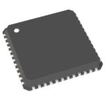 AD9524BCPZ-REEL7
The activity of extra discounts on wholesale prices is in full swing…
Please fill in your contact information and we will send you the latest wholesale price list.






