 ChipApex | Global Electronic Components Supplier
AD9531BCPZ-REEL7
Search Product
Search Post
— IC芯片 | 连接器 | 传感器 | 被动器件 —
Search productSearch post
— IC芯片 | 连接器 | 传感器 | 被动器件 —
Consult the customer manager about the wholesale price.
consultation hotline:86-132-6715-2157
email:[email protected]
Contact the product manager for consultation. One-stop consultation is available.
Do you want a lower wholesale price? Please send us your inquiry and we will reply immediately.
The AD9531BCPZ-REEL7 is a three-channel clock generator and baseband clock distributor from Analog Devices, housed in an 88-lead LFCSP package. It integrates three PLL/VCO cores (PLL1, PLL2, PLL3) to provide 24 outputs with typical jitter performance of 0.462 ps rms. The device supports input frequencies ranging from 9.5 MHz to 260 MHz and generates output frequencies up to 400 MHz. It operates on 3.3 V and 1.8 V supplies within a temperature range of −40°C to +85°C.
Verify component authenticity through authorized distributors or the manufacturer directly. Confirm the specific REEL7 packaging suffix matches system requirements. Check current availability status as supply conditions may vary. Ensure compliance with RoHS directives and environmental regulations relevant to the deployment region.
Select this component when multiple low-jitter clock domains are required from a single source. Verify that the input frequency range (9.5 MHz to 260 MHz) aligns with the reference source. Ensure the target output frequencies do not exceed 400 MHz. Consider the 88-lead LFCSP thermal characteristics and PCB layout constraints during design.
This part belongs to the AD9531 series of multi-output clock generators. It is designed for high-performance timing applications requiring precise phase relationships between multiple outputs. The device replaces discrete clock distribution solutions by integrating multiple PLLs and output drivers into a single compact package.
Publicly confirmed substitute part numbers are not available in the provided documentation. Evaluate alternative Analog Devices clock generators based on channel count, jitter specifications, and package compatibility if replacement is necessary.
The AD9531 supports output frequencies up to 400 MHz across its various output channels.
Yes, PLL1 can operate with an external voltage controlled crystal oscillator (VCXO) instead of the internal VCO.
The typical absolute time jitter for PLL1 in fractional-N mode is 0.462 ps rms.
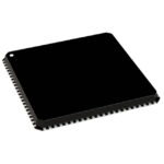 AD9531BCPZ-REEL7
The activity of extra discounts on wholesale prices is in full swing…
Please fill in your contact information and we will send you the latest wholesale price list.






