 ChipApex | Global Electronic Components Supplier
AD9549BCPZ
Search Product
Search Post
— IC芯片 | 连接器 | 传感器 | 被动器件 —
Search productSearch post
— IC芯片 | 连接器 | 传感器 | 被动器件 —
Consult the customer manager about the wholesale price.
consultation hotline:86-132-6715-2157
email:[email protected]
Contact the product manager for consultation. One-stop consultation is available.
Do you want a lower wholesale price? Please send us your inquiry and we will reply immediately.
The AD9549BCPZ is a dual-input network clock generator and synchronizer in a 64-lead LFCSP package. It accepts reference inputs from 8 kHz to 750 MHz and generates synchronized output clocks up to 750 MHz. Key specifications include a digital PLL with programmable loop filters, a high-speed digitally controlled oscillator (DCO) core, and an integrated direct digital synthesizer (DDS) with a 14-bit DAC. The device supports smooth A-to-B phase transitions, auto/manual holdover modes, and loss of reference indicators. Operating temperatures range from -40°C to +85°C.
Verify the specific ordering suffix against the manufacturer's current documentation to confirm package type and temperature grade. Confirm availability status through authorized distributors as supply levels fluctuate. Ensure proper ESD handling protocols are followed during storage and assembly due to the sensitivity of the CMOS components.
Select this component when dual-reference redundancy and low-jitter holdover capabilities are required. Verify that the input signal slew rate meets the minimum specification of 40 V/μs for optimal performance. Ensure the system design accommodates the necessary external loop filter components for the DCO and DAC feedback paths.
The AD9549 belongs to Analog Devices' family of network clock generators designed for high-performance synchronization. It complements other devices like the AD9546 and AD9547 by offering specific features such as an integrated DDS and dual reference inputs. It is commonly used in telecommunications infrastructure requiring precise timing alignment.
The AD9546BCPZ serves as a related alternative within the same product family, though it offers different output configurations and pin counts. Verify functional compatibility regarding interface requirements and output drive capabilities before substitution.
The single-ended CMOS output driver supports frequencies up to 150 MHz when powered at 3.3 V.
The AD9549 provides loss of reference indicators and supports both auto and manual holdover modes to maintain a valid output clock even if both references fail.
The device operates over an industrial temperature range of -40°C to +85°C.
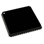 AD9549BCPZ
The activity of extra discounts on wholesale prices is in full swing…
Please fill in your contact information and we will send you the latest wholesale price list.





