 ChipApex | Global Electronic Components Supplier
SEARCH
Search Product
Search Post
— IC芯片 | 连接器 | 传感器 | 被动器件 —
Search productSearch post
— IC芯片 | 连接器 | 传感器 | 被动器件 —
Consult the customer manager about the wholesale price.
consultation hotline:86-132-6715-2157
email:[email protected]
Contact the product manager for consultation. One-stop consultation is available.
Do you want a lower wholesale price? Please send us your inquiry and we will reply immediately.
The AD9842AJST is a complete analog signal processor for CCD applications, featuring a single-channel architecture designed to sample and condition outputs of interlaced and progressive scan area CCD arrays. It operates from a single 3 V power supply with typical power consumption of 78 mW. The device includes a 12-bit A/D converter with a maximum clock rate of 20 MHz. Key specifications include an operating temperature range of -20°C to +85°C, a 48-lead LQFP package, and a 3-wire serial digital interface for register programming.
Verify the component against official Analog Devices documentation to confirm pinout compatibility and electrical characteristics. Ensure that the specific ordering suffix matches the required package type and temperature range. Cross-reference the manufacturer part number with authorized distributors to validate authenticity and traceability before integration into designs.
Select this model when a 12-bit ADC resolution is required for CCD signal processing at speeds up to 20 MSPS. Consider the AD9841A variant if 10-bit resolution is sufficient for the application. Evaluate the 48-lead LQFP package constraints and verify that the 3 V single-supply operation aligns with the system power budget and thermal requirements.
The AD9842AJST belongs to the AD9841A/AD9842A family of complete CCD signal processors manufactured by Analog Devices. This series provides integrated analog front-end solutions specifically tailored for imaging applications requiring high-speed sampling and precise signal conditioning of CCD array outputs.
The AD9841AJST is a direct functional substitute within the same family, differing only in ADC resolution (10-bit vs. 12-bit). Verify that the reduced resolution meets the system requirements before substitution.
The primary difference is the ADC resolution; the AD9841A features a 10-bit A/D converter, while the AD9842A contains a true 12-bit A/D converter. Both share the same 20 MSPS architecture and peripheral features.
The Pixel Gain Amplifier (PxGA) gain is controlled via a 6-bit digital value loaded through the 3-wire serial interface. It supports four separate gain values that can be multiplexed on a pixel-to-pixel basis using the Color Steering modes.
CLPOB (Black Level Clamp Clock) and CLPDM (Input Clamp Clock) are used to control the low noise clamp circuits. They remove DC offsets from the CCD signal, such as optical black levels, during specific phases of the line timing.
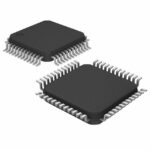 AD9842AJST
The activity of extra discounts on wholesale prices is in full swing…
Please fill in your contact information and we will send you the latest wholesale price list.





