 ChipApex | Global Electronic Components Supplier
SEARCH
Search Product
Search Post
— IC芯片 | 连接器 | 传感器 | 被动器件 —
Search productSearch post
— IC芯片 | 连接器 | 传感器 | 被动器件 —
Consult the customer manager about the wholesale price.
consultation hotline:86-132-6715-2157
email:[email protected]
Contact the product manager for consultation. One-stop consultation is available.
Do you want a lower wholesale price? Please send us your inquiry and we will reply immediately.
The AD9945KCPRL is a complete analog signal processor for CCD applications, featuring a 40 MHz single-channel architecture. It integrates a correlated double sampler (CDS), a digitally controlled variable gain amplifier (VGA) with 6 dB to 40 dB range, an optical black clamp circuit, and a 12-bit A/D converter. The device operates from a single 3 V supply, dissipating 160 mW in normal operation and 1.5 mW in power-down mode. Internal registers are programmed via a 3-wire serial interface supporting up to 10 MHz SCK frequency. It functions within a temperature range of -20°C to +85°C and utilizes a 32-lead LFCSP package.
Verify the specific ordering suffix against the manufacturer's current documentation to confirm package type and RoHS compliance status. Confirm that the component meets the required operating temperature range and voltage specifications for the target application environment before finalizing procurement decisions.
Select this component when a single-chip solution for CCD signal processing is required. Ensure the system timing generator can provide the necessary SHP, SHD, and DATACLK signals. Verify that the external coupling capacitor matches the DC restore requirements and that the digital interface logic levels are compatible with the host controller.
The AD9945 serves as a dedicated analog front-end processor for area CCD arrays. It consolidates multiple signal conditioning stages into one package, reducing board space and design complexity. The device is designed to interface directly with CCD outputs, handling DC restoration, noise reduction, gain adjustment, and digitization in a unified workflow.
The AD9945KCPZ is a verified equivalent part number offering identical functionality and pinout compatibility. Both variants share the same electrical characteristics and package dimensions, allowing for direct substitution in existing designs without hardware modifications.
During power-up, the value 0x838 must be written into Register 0xD to ensure proper start-up operation of the internal circuits.
The VGA gain in decibels is calculated using the formula: Gain (dB) = (VGA Code Value × 0.035 dB) + 5.3 dB.
The CLPOB pulse triggers the optical black clamp loop during the CCD's optical black pixel interval to remove residual offsets and track low-frequency black level variations.
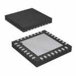 AD9945KCPRL
The activity of extra discounts on wholesale prices is in full swing…
Please fill in your contact information and we will send you the latest wholesale price list.





