ChipApex | Global Electronic Components Supplier
ADA4800ACPZ-R7
Search Product
Search Post
— IC芯片 | 连接器 | 传感器 | 被动器件 —
Search productSearch post
— IC芯片 | 连接器 | 传感器 | 被动器件 —
Consult the customer manager about the wholesale price.
consultation hotline:86-132-6715-2157
email:[email protected]
Contact the product manager for consultation. One-stop consultation is available.
Do you want a lower wholesale price? Please send us your inquiry and we will reply immediately.
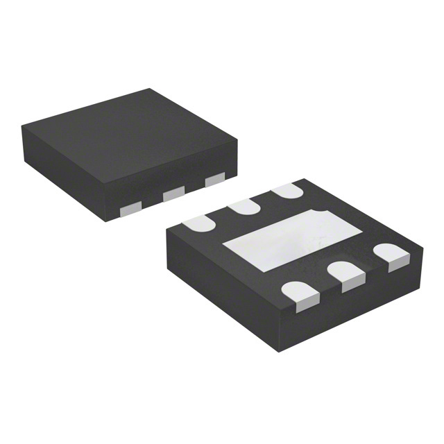
The ADA4800ACPZ-R7 is a low power, high speed CCD buffer amplifier manufactured by Analog Devices Inc. It integrates an active load with a unity gain voltage buffer in a 6-lead LFCSP package. The device operates on supply voltages ranging from 4 V to 17 V and functions within an industrial temperature range of -40°C to +85°C. Key electrical specifications include a maximum slew rate of 415 V/μs and a typical -3 dB bandwidth of 400 MHz when configured for optimal performance. The input bias current is specified at 1 μA, while the quiescent supply current is approximately 1.4 mA. The output stage utilizes a push-pull architecture to provide drive capability for both rising and falling signal transitions.
Verify the specific ordering suffix corresponds to the required tape and reel quantity configuration. Confirm RoHS compliance status matches project environmental requirements. Ensure the LFCSP-6 footprint dimensions align with the PCB layout guidelines provided in the datasheet outline drawing. Validate that the operating temperature range meets the intended application environment constraints.
Select this component when driving open-source CCD sensors requiring integrated active loading. Consider the adjustable bandwidth feature if system noise or stability requires tuning the frequency response. Evaluate the power save functionality if standby current reduction is critical. Ensure the supply voltage range accommodates the specific sensor and analog front-end interface requirements.
This part belongs to the ADA4800 series of charge-coupled device buffer amplifiers. It is designed specifically for applications requiring low power consumption alongside high-speed signal integrity. The integration of the active load simplifies the external circuit design compared to discrete solutions. It serves as an interface between CCD outputs and subsequent analog-to-digital conversion stages.
ADA4800ACPZ-R2
The bandwidth is controlled by connecting an external resistor between the IDRV pin and a voltage source (such as VCC). Adjusting this resistance changes the quiescent current (ICC), which directly influences the -3 dB bandwidth.
The ISF pin sets the value of the active current load (IAL) connected to the input. It can also be used to enable a power save mode by disconnecting the active load current when a logic low or negative voltage is applied.
Yes, the active load current can be switched off using the ISF pin while the buffer continues to operate as a standard unity gain amplifier. This allows the device to function solely as a buffer without loading the sensor.
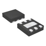 ADA4800ACPZ-R7
The activity of extra discounts on wholesale prices is in full swing…
Please fill in your contact information and we will send you the latest wholesale price list.