ChipApex | Global Electronic Components Supplier
ADA4817-1ACPZ-R2
Search Product
Search Post
— IC芯片 | 连接器 | 传感器 | 被动器件 —
Search productSearch post
— IC芯片 | 连接器 | 传感器 | 被动器件 —
Consult the customer manager about the wholesale price.
consultation hotline:86-132-6715-2157
email:[email protected]
Contact the product manager for consultation. One-stop consultation is available.
Do you want a lower wholesale price? Please send us your inquiry and we will reply immediately.
The ADA4817-1ACPZ-R2 is a single-channel, unity-gain stable, ultrahigh-speed voltage feedback operational amplifier with FET inputs. It features a -3 dB bandwidth of 1050 MHz at G=1 and RL=100 Ω, a slew rate of 870 V/µs, and a 0.1% settling time of 9 ns. Input noise is 4 nV/√Hz voltage and 2.5 fA/√Hz current at 100 kHz. The device operates on supply voltages from 5 V to 10 V, drawing 19 mA quiescent current per amplifier. It includes a power-down pin reducing current to 1.5 mA. The component is housed in an 8-lead LFCSP package rated for operation between -40°C and +105°C.
Verify the specific ordering suffix ACPZ-R2 against the manufacturer's official ordering guide to confirm the package type and reel quantity. Ensure the procurement source provides valid traceability documentation. Confirm that the received components match the Rev. I datasheet specifications. Check for any product change notifications that may affect performance or reliability parameters prior to final integration.
Select this amplifier for applications requiring ultrahigh speed combined with low noise characteristics. The FET input stage offers very high input impedance suitable for sensitive signal sources. Consider the thermal resistance of the exposed pad for heat dissipation in dense layouts. Verify that the required supply voltage range fits within the 5 V to 10 V operating limits. Evaluate the need for the power-down feature if system power management is critical.
Analog Devices manufactures the ADA4817 series using its proprietary XFCB process technology. This family includes single and dual channel variants designed for wideband transimpedance and data acquisition applications. The devices are engineered to balance high slew rates with minimal input capacitance, addressing the needs of modern high-resolution instrumentation systems.
Consult the official Analog Devices ordering guide for verified substitute part numbers. Cross-reference pinouts and electrical specifications carefully before substitution.
The amplifier is enabled when the PD pin voltage is within 0.9 V of the positive supply rail. It enters power-down mode when the PD pin voltage is at least 3.5 V below the positive supply, reducing quiescent current to approximately 1.5 mA.
Feedback resistances between 100 Ω and 400 Ω are recommended to minimize peaking in the frequency response without degrading the output stage performance.
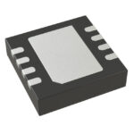 ADA4817-1ACPZ-R2
The activity of extra discounts on wholesale prices is in full swing…
Please fill in your contact information and we will send you the latest wholesale price list.