ChipApex | Global Electronic Components Supplier
ADA4930-1YCPZ-R7
Search Product
Search Post
— IC芯片 | 连接器 | 传感器 | 被动器件 —
Search productSearch post
— IC芯片 | 连接器 | 传感器 | 被动器件 —
Consult the customer manager about the wholesale price.
consultation hotline:86-132-6715-2157
email:[email protected]
Contact the product manager for consultation. One-stop consultation is available.
Do you want a lower wholesale price? Please send us your inquiry and we will reply immediately.
The ADA4930-1YCPZ-R7 is a single-channel ultralow noise differential amplifier in a 16-lead LFCSP package. It operates on a single 3.3 V or 5 V supply with a quiescent current of approximately 34 mA per amplifier. Key electrical parameters include a small-signal bandwidth of 1.35 GHz, a slew rate of 3400 V/μs, and an input voltage noise density of 1.2 nV/√Hz at 5 V operation. The device features adjustable output common-mode voltage via the VOCM pin and supports gains set by external feedback resistors.
Verify the specific ordering suffix R7 corresponds to reel packaging when sourcing. Confirm the component matches the 16-lead LFCSP physical footprint and pinout defined in the datasheet. Ensure the supply voltage requirements align with the 3.3 V or 5 V operational specifications provided in the official documentation.
Select this component for applications requiring high speed and low noise in a compact surface-mount package. The single-channel architecture suits designs needing one differential driver. Consider the 1.35 GHz bandwidth and 3400 V/μs slew rate for high-frequency signal integrity. Verify that the required gain settings can be achieved with available external resistor values within the specified input resistance limits.
This part belongs to the ADA4930 family of ultralow noise drivers designed specifically for low voltage ADCs. The -1 suffix indicates a single-channel configuration, distinguishing it from the dual-channel ADA4930-2. Manufactured using a silicon-germanium complementary bipolar process, the device optimizes PCB layout to minimize distortion while maintaining high dynamic performance.
The ADA4930-2 serves as the dual-channel counterpart within the same family. Designers requiring two channels may consider this alternative if the board space allows for the 24-lead LFCSP package. No other direct substitutes are confirmed in the provided documentation.
The output common-mode voltage is adjusted by applying a voltage to the VOCM pin. An internal common-mode feedback loop forces the output common-mode level to match the voltage applied to this input.
The typical input offset voltage is 0.5 mV, with a maximum specified drift of 2.75 μV/°C across the operating temperature range.
Yes, the ADA4930-1 includes a Power-Down (PD) pin. Driving this pin low disables the amplifier, reducing the quiescent current significantly compared to the enabled state.
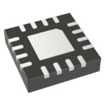 ADA4930-1YCPZ-R7
The activity of extra discounts on wholesale prices is in full swing…
Please fill in your contact information and we will send you the latest wholesale price list.