 ChipApex | Global Electronic Components Supplier

SEARCH
Search Product
Search Post
— IC芯片 | 连接器 | 传感器 | 被动器件 —
Search productSearch post
— IC芯片 | 连接器 | 传感器 | 被动器件 —
Consult the customer manager about the wholesale price.
consultation hotline:86-132-6715-2157
email:[email protected]
Contact the product manager for consultation. One-stop consultation is available.
Do you want a lower wholesale price? Please send us your inquiry and we will reply immediately.
ADCLK854BCPZ is listed in the Clock Buffers, Drivers range at ChipApex. The manufacturer field lists Analog Devices Inc.. Its product description is IC CLK BUF 2:12 1.2GHZ 48LFCSP. Review the specifications below when checking this part for your BOM.
The ADCLK854BCPZ is a low-power clock fanout buffer from Analog Devices, housed in a 48-pin LFCSP package. It features two selectable differential inputs and supports up to 12 LVDS outputs at 1.2 GHz or 24 CMOS outputs at 250 MHz. The device operates on a 1.8 V supply (1.71 V to 1.89 V) within an industrial temperature range of -40°C to +85°C. Key electrical specifications include 54 fs rms integrated jitter (12 kHz to 20 MHz), 100 fs rms additive broadband jitter, and a typical propagation delay of 2.0 ns for LVDS outputs.
Verify the specific suffix 'BCPZ' against the manufacturer's ordering guide to confirm package type (LFCSP-48) and temperature grade. Ensure the procurement source provides the official datasheet Rev. A for accurate timing and electrical characteristics. Confirm RoHS compliance status as indicated in the product documentation.
Select this component when a single buffer must drive mixed LVDS and CMOS loads simultaneously. The device allows independent configuration of three output banks (four outputs each). Ensure the input signal slew rate exceeds 1 V/ns to maintain optimal jitter performance. Verify that the PCB layout accommodates the exposed paddle thermal connection to ground.
The ADCLK854BCPZ belongs to the ADCLK854 series of clock buffers. It is designed to replace discrete buffering solutions by integrating multiple driver types into one chip. The part is optimized for applications requiring high fan-out ratios with minimal added jitter, serving as a central distribution point for high-speed digital systems.
Public confirmed substitute part numbers are not available in the provided documentation. Check the manufacturer's ordering guide for any updated revisions or alternative packages within the same family before substitution.
The outputs are grouped into three banks of four. The CTRL_A, CTRL_B, and CTRL_C pins determine whether each bank operates as LVDS (logic low) or CMOS (logic high).
The device supports a maximum differential input frequency of 1.2 GHz for LVDS outputs and 250 MHz for CMOS outputs.
Pulling the SLEEP pin high activates sleep mode, which powers down the device except for the internal bandgap and places all outputs in a high-Z state.
Explore related parts through Clock/Timing, Integrated Circuits (ICs), all product categories, ChipApex homepage.
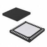 ADCLK854BCPZ

The activity of extra discounts on wholesale prices is in full swing…
Please fill in your contact information and we will send you the latest wholesale price list.






