 ChipApex | Global Electronic Components Supplier
SEARCH
Search Product
Search Post
— IC芯片 | 连接器 | 传感器 | 被动器件 —
Search productSearch post
— IC芯片 | 连接器 | 传感器 | 被动器件 —
Consult the customer manager about the wholesale price.
consultation hotline:86-132-6715-2157
email:[email protected]
Contact the product manager for consultation. One-stop consultation is available.
Do you want a lower wholesale price? Please send us your inquiry and we will reply immediately.
The ADD8506WRUZ-REEL7 is a 6-channel LCD gamma reference buffer manufactured by Analog Devices Inc. It operates on a single supply voltage ranging from 3.3 V to 6.5 V and features rail-to-rail input and output capabilities. The device provides a high output current of 380 mA and maintains a low supply current of 3.9 mA. It is designed to be stable with loads up to 1 nF and functions within a temperature range of −40°C to +105°C. The component is housed in a 24-lead Thin Shrink Small Outline Package (TSSOP) and is supplied in a 7-inch tape and reel format.
Verify that the specific part number matches the required package type and quantity, as the suffix indicates a 7-inch tape and reel configuration. Confirm the operating temperature range aligns with system requirements. Check for any automotive qualification needs, noting that the standard commercial version differs from the qualified automotive model. Ensure the RoHS compliance status meets environmental standards for the intended deployment.
Select this component when driving column drivers in line inversion LCD panels requiring six independent gamma buffers. Consider the high output current capability for driving resistive or capacitive loads directly without series resistors. Evaluate the low supply current for power-sensitive applications. Verify that the 24-lead TSSOP package fits the PCB layout constraints and thermal management requirements of the design.
This device belongs to the ADD8504/ADD8505/ADD8506 family of LCD gamma reference buffers. While the ADD8504 offers four channels and the ADD8505 offers five, the ADD8506 provides six channels to support larger displays. All models share similar electrical characteristics, including rail-to-rail operation and high slew rates, but differ in pin count and channel density within the same TSSOP package family.
The ADD8506WWARUZR7 is the automotive-grade equivalent of the ADD8506WRUZ-REEL7. Designers should verify if automotive reliability reports are necessary for their application. No other direct functional substitutes are listed in the provided documentation.
The A/B input acts as a switch control where a logic high selects Input A (INAx) and a logic low selects Input B (INBx), allowing the selection between two different gamma voltage curves set by external resistor ladders.
Because the buffers deliver high peak currents, it is recommended that all GND and VCC pins be connected and suitably bypassed to ensure stable operation.
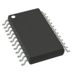 ADD8506WRUZ-REEL
The activity of extra discounts on wholesale prices is in full swing…
Please fill in your contact information and we will send you the latest wholesale price list.





