 ChipApex | Global Electronic Components Supplier
ADF4001BRU
Search Product
Search Post
— IC芯片 | 连接器 | 传感器 | 被动器件 —
Search productSearch post
— IC芯片 | 连接器 | 传感器 | 被动器件 —
Consult the customer manager about the wholesale price.
consultation hotline:86-132-6715-2157
email:[email protected]
Contact the product manager for consultation. One-stop consultation is available.
Do you want a lower wholesale price? Please send us your inquiry and we will reply immediately.
The ADF4001BRU is a 200 MHz bandwidth integer-N clock generator PLL from Analog Devices, housed in a 16-lead TSSOP package. It operates on a single supply voltage ranging from 2.7 V to 5.5 V, with a typical operating current of 4.5 mA. The device integrates a low-noise digital phase frequency detector (PFD), a precision charge pump, a programmable 13-bit N counter, and a 14-bit R counter. It features a separate charge pump supply pin (VP) to support extended tuning voltages up to 6.0 V in 5 V systems. The component utilizes a 3-wire serial interface for configuration and supports hardware and software power-down modes.
Verify the specific suffix 'BRU' corresponds to the tube packaging variant rather than the reel or cut tape options. Confirm that the B-version industrial temperature range (-40°C to +85°C) meets system requirements. Ensure the 16-lead TSSOP footprint matches the PCB layout design. Check for RoHS compliance status as indicated in official documentation.
Select this component when a low-noise integer-N synthesizer is required for frequencies up to 200 MHz. The separate VP supply is critical if the external VCO requires a tuning voltage exceeding the logic supply voltage. Ensure the available charge pump currents (ranging from ~0.3 mA to ~5 mA depending on RSET) are sufficient for the external loop filter design. Verify compatibility with existing microcontroller serial interfaces for the 3-wire control protocol.
The ADF4001 belongs to the ADF4001 family of clock generators designed for low-frequency PLL applications. It serves as a core synthesizer component that requires an external voltage-controlled oscillator (VCO) or voltage-controlled crystal oscillator (VCXO) and an external loop filter to function as a complete phase-locked loop. The BRU designation specifically identifies the 16-lead TSSOP package version of this integrated circuit.
The datasheet explicitly states hardware compatibility with the ADF4110, ADF4111, ADF4112, and ADF4113 models. These parts share similar functional latch structures and pinouts, allowing for potential direct replacements in designs utilizing those specific variants.
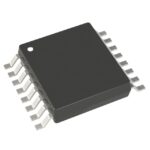 ADF4001BRU
The activity of extra discounts on wholesale prices is in full swing…
Please fill in your contact information and we will send you the latest wholesale price list.





