 ChipApex | Global Electronic Components Supplier
ADF4001SP1BRU-RL7
Search Product
Search Post
— IC芯片 | 连接器 | 传感器 | 被动器件 —
Search productSearch post
— IC芯片 | 连接器 | 传感器 | 被动器件 —
Consult the customer manager about the wholesale price.
consultation hotline:86-132-6715-2157
email:[email protected]
Contact the product manager for consultation. One-stop consultation is available.
Do you want a lower wholesale price? Please send us your inquiry and we will reply immediately.
The ADF4001SP1BRU-RL7 is a clock generator PLL from Analog Devices, part of the ADF4001 series. It features a 200 MHz bandwidth and operates on a 2.7 V to 5.5 V power supply. The device includes separate charge pump supply (VP) for extended tuning voltage in 5 V systems, programmable charge pump currents, and a 3-wire serial interface. Typical operating current is 4.5 mA with ultralow phase noise. It is housed in a 16-lead TSSOP package.
Verify the specific suffix 'SP1B' against official Analog Devices documentation to confirm pinout, temperature range, or packaging variations compared to standard ADF4001 variants. Ensure compatibility with existing board layouts when substituting.
Select this component for applications requiring stable reference signals with low noise. Consider the 2.7 V to 5.5 V supply range and 4.5 mA typical current consumption. Verify that the 16-lead TSSOP package fits the design constraints.
The ADF4001 series is designed for implementing clock sources for PLLs requiring very low noise, stable reference signals. It consists of a low noise digital PFD, precision charge pump, programmable reference divider, and programmable 13-bit N counter.
Standard ADF4001 variants such as ADF4001BCPZ or ADF4001BRU may be functionally similar but differ in package (LFCSP vs TSSOP). Verify electrical specifications and pin compatibility before substitution.
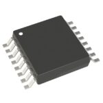 ADF4001SP1BRU-RL7
The activity of extra discounts on wholesale prices is in full swing…
Please fill in your contact information and we will send you the latest wholesale price list.






