 ChipApex | Global Electronic Components Supplier
ADF4111BRU
Search Product
Search Post
— IC芯片 | 连接器 | 传感器 | 被动器件 —
Search productSearch post
— IC芯片 | 连接器 | 传感器 | 被动器件 —
Consult the customer manager about the wholesale price.
consultation hotline:86-132-6715-2157
email:[email protected]
Contact the product manager for consultation. One-stop consultation is available.
Do you want a lower wholesale price? Please send us your inquiry and we will reply immediately.
The ADF4111BRU is an RF PLL frequency synthesizer from Analog Devices, designed for local oscillator implementation in wireless transceivers. It supports a maximum RF input frequency of 1.2 GHz and operates on a 2.7 V to 5.5 V power supply. The device integrates a low-noise digital phase frequency detector, a precision charge pump with programmable currents, and a programmable reference divider. Key specifications include a typical operating current of 4.5 mA at 5 V and an industrial temperature range of -40°C to +85°C. It utilizes a 3-wire serial interface for register control and offers hardware and software power-down modes.
Verify the package type matches the design requirements, as the ADF4111 family is available in TSSOP-16 and LFCSP packages. Confirm that the specific suffix indicates the correct temperature grade and packaging format. Ensure the ordering information aligns with the manufacturer's current documentation to avoid discrepancies in electrical characteristics or pinout definitions.
Select the ADF4111 when the application requires a frequency synthesizer with an RF input range extending up to 1.2 GHz. Consider this component if the system design benefits from a separate charge pump supply (VP) to support higher VCO tuning voltages in 3 V systems. Verify that the required division ratios can be achieved using the programmable A and B counters in conjunction with the selected prescaler modulus.
The ADF4111 is part of the ADF4110 family, which includes the ADF4110, ADF4112, and ADF4113. These devices share similar architectures and pinouts but differ primarily in their maximum RF input frequencies, ranging from 550 MHz to 4.0 GHz. This family is designed for compatibility within wireless communication systems requiring integer-N frequency synthesis.
The ADF4110, ADF4112, and ADF4113 are pin-compatible alternatives within the same family. Selection among these depends on whether the specific RF frequency requirement is below 550 MHz, between 550 MHz and 1.2 GHz, or above 1.2 GHz up to 4.0 GHz.
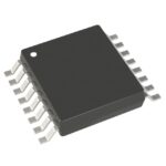 ADF4111BRU
The activity of extra discounts on wholesale prices is in full swing…
Please fill in your contact information and we will send you the latest wholesale price list.





