 ChipApex | Global Electronic Components Supplier
ADF4212LBRUZ
Search Product
Search Post
— IC芯片 | 连接器 | 传感器 | 被动器件 —
Search productSearch post
— IC芯片 | 连接器 | 传感器 | 被动器件 —
Consult the customer manager about the wholesale price.
consultation hotline:86-132-6715-2157
email:[email protected]
Contact the product manager for consultation. One-stop consultation is available.
Do you want a lower wholesale price? Please send us your inquiry and we will reply immediately.
The ADF4212LBRUZ is a dual low-power PLL frequency synthesizer from Analog Devices, housed in a 20-lead TSSOP package. It integrates two independent synthesizers for RF and IF sections, supporting input frequencies up to 2.4 GHz (RF) and 1.0 GHz (IF). The device operates on a 2.7 V to 3.3 V supply with a typical current consumption of 7.5 mA. Key features include programmable dual modulus prescalers (8/9, 16/17, 32/33, 64/65), a 3-wire serial interface, and separate VP supplies allowing extended tuning voltages up to 5.5 V. It supports integer-N synthesis via internal A, B, and R counters.
Verify the specific ordering suffix against the manufacturer's current data sheet to confirm package type and tape/reel specifications. The 'BRUZ' designation indicates a 20-lead TSSOP package. Confirm RoHS compliance status and lead-free soldering requirements with the supplier prior to procurement.
Select this component when dual independent frequency synthesizers are required within a single chip footprint. Ensure the external VCO tuning voltage does not exceed the VP pin maximum rating of 5.5 V. Verify that the desired reference frequency falls within the 10 MHz to 150 MHz range and that the prescaler setting allows the input frequency to be divided below the 188 MHz CMOS counter limit.
The ADF4212L belongs to the ADF4212 family of dual PLL synthesizers. The BRUZ variant specifically denotes the 20-lead Thin Shrink Small Outline Package (TSSOP). Other variants in the family may offer different packaging options such as the LFCSP or different electrical grade suffixes.
Direct replacements within the same series include other ADF4212 variants with different package codes (e.g., ADF4212BCPZ for LFCSP). Cross-family alternatives require verification of pin compatibility and electrical parameter alignment with the original design requirements.
The maximum operating frequency of the CMOS counters (prescaler output) is 188 MHz. The prescaler value must be selected to ensure the divided RF/IF input frequency remains below this limit.
The charge pump current is set by connecting a resistor between the RSET pin and ground. The relationship is defined as ICP_MAX = 13.5 / RSET. For example, a 2.7 kΩ resistor yields a typical maximum current of 5 mA.
Yes, VDD1 and VDD2 must have the same potential (2.7 V to 3.3 V). However, the VP1 and VP2 pins can be supplied with a higher voltage (up to 5.5 V) to drive VCOs requiring extended tuning ranges.
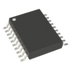 ADF4212LBRUZ
The activity of extra discounts on wholesale prices is in full swing…
Please fill in your contact information and we will send you the latest wholesale price list.





