 ChipApex | Global Electronic Components Supplier
ADF4252BCPZ-R7
Search Product
Search Post
— IC芯片 | 连接器 | 传感器 | 被动器件 —
Search productSearch post
— IC芯片 | 连接器 | 传感器 | 被动器件 —
Consult the customer manager about the wholesale price.
consultation hotline:86-132-6715-2157
email:[email protected]
Contact the product manager for consultation. One-stop consultation is available.
Do you want a lower wholesale price? Please send us your inquiry and we will reply immediately.
The ADF4252BCPZ-R7 is a dual fractional-N/integer-N frequency synthesizer manufactured by Analog Devices Inc. It integrates two independent synthesizers: an RF section supporting up to 3 GHz with fractional-N capabilities, and an IF section operating up to 1.2 GHz using integer-N division. The device operates on a 2.7 V to 3.3 V supply and features separate power pins (VP1, VP2) allowing extended tuning voltages up to 5.5 V. Key specifications include a programmable dual modulus prescaler, digital lock detect, and a 3-wire serial interface for register control.
Verify the component matches the LFCSP-24 package and Rev E datasheet specifications. Confirm that the RSET resistor value aligns with the required minimum charge pump current, as the internal reference sets ICP_MIN = 1.6875/RSET. Ensure proper decoupling of VDD1, VDD2, VDD3, and DVDD pins to the ground plane during assembly.
Select this component when a single IC must provide both high-frequency fractional-N synthesis for RF local oscillators and lower-frequency integer-N synthesis for IF stages. The device requires external loop filters and voltage-controlled oscillators (VCOs) to complete the phase-locked loops. Designers should account for the separate analog and digital ground planes (AGND and DGND) to minimize noise coupling between the RF and IF sections.
This part belongs to the ADF4252 series of dual synthesizers from Analog Devices. It is designed to replace discrete PLL solutions in compact wireless designs. The 'R7' suffix indicates tape and reel packaging. The device is distinct from single-loop synthesizers like the ADF41020 or integrated VCO synthesizers like the ADF4350.
Public confirmed substitute part numbers are not available in the provided documentation. Designers should verify pin compatibility and electrical parameters if considering alternative dual-synthesizer ICs from other manufacturers.
The RF input frequency (RFINA, RFINB) supports up to 3.0 GHz, while the IF input frequency (IFINA, IFINB) supports up to 1.2 GHz.
The minimum charge pump current is set by an external resistor connected to the RSET pin. The relationship is defined as ICP_MIN = 1.6875 / RSET, where RSET is in kΩ and ICP_MIN is in mA.
Yes, the device contains two independent synthesizers. However, they share the same power supply rails (VDD1-VDD3) and reference input (REFIN), requiring careful power management and filtering design.
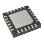 ADF4252BCPZ-R7
The activity of extra discounts on wholesale prices is in full swing…
Please fill in your contact information and we will send you the latest wholesale price list.






