 ChipApex | Global Electronic Components Supplier
ADF4360-8BCPRL
Search Product
Search Post
— IC芯片 | 连接器 | 传感器 | 被动器件 —
Search productSearch post
— IC芯片 | 连接器 | 传感器 | 被动器件 —
Consult the customer manager about the wholesale price.
consultation hotline:86-132-6715-2157
email:[email protected]
Contact the product manager for consultation. One-stop consultation is available.
Do you want a lower wholesale price? Please send us your inquiry and we will reply immediately.
The ADF4360-8BCPRL is an integrated integer-N synthesizer and voltage-controlled oscillator (VCO) manufactured by Analog Devices Inc. It operates within a frequency range of 65 MHz to 400 MHz, determined by external inductors connected to the L1 and L2 pins. The device supports a power supply voltage between 3.0 V and 3.6 V and features 1.8 V logic compatibility. Control registers are accessed via a simple 3-wire serial interface comprising CLK, DATA, and LE inputs. Key specifications include a programmable output power level ranging from -9 dBm to 0 dBm, digital lock detect functionality, and hardware/software power-down modes for energy efficiency.
Verify the specific suffix 'RL' against the manufacturer's official ordering guide to confirm packaging details such as reel quantity or tape-and-reel configuration. Ensure the component matches the B version electrical characteristics defined in the datasheet. Confirm that the package type corresponds to the Chip Scale Package (CSP) outline dimensions provided in the documentation.
Select appropriate external inductors for the L1 and L2 pins to set the desired center frequency within the 65 MHz to 400 MHz range. Ensure the reference input frequency does not exceed 250 MHz and that the R counter division allows the PFD frequency to remain below 8 MHz. Verify that the charge pump current setting via RSET and CPI bits meets the loop filter design requirements for stability.
The ADF4360-8 belongs to the ADF4360 family of integrated synthesizers and VCOs. This family includes variants with different fixed frequency ranges, such as the ADF4360-0 (2.4 GHz–3.0 GHz) and ADF4360-3 (1.6 GHz–1.95 GHz). The ADF4360-8 is distinct due to its lower frequency range enabled by external inductors, making it suitable for applications requiring frequencies below 400 MHz.
For direct replacements within the same family, consider the ADF4360-8BCPZ (tray package) if reel packaging is not required. Other ADF4360 variants like the ADF4360-0 or ADF4360-3 offer different frequency ranges and are not electrically compatible without significant circuit redesign.
The output frequency range of 65 MHz to 400 MHz is set by connecting external inductors to the L1 and L2 pins. These inductors must be of equal value and connected to AGND.
The CE (Chip Enable) pin controls the power state. A logic low powers down the device and puts the charge pump into three-state mode. A logic high powers up the device according to the status of the power-down bits in the control latch.
The maximum charge pump current is set by the resistor connected between the RSET pin and CPGND. Additionally, the CP gain can be fine-tuned using the CPI1 through CPI6 bits in the control latch.
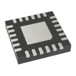 ADF4360-8BCPRL
The activity of extra discounts on wholesale prices is in full swing…
Please fill in your contact information and we will send you the latest wholesale price list.





