 ChipApex | Global Electronic Components Supplier

SEARCH
Search Product
Search Post
— IC芯片 | 连接器 | 传感器 | 被动器件 —
Search productSearch post
— IC芯片 | 连接器 | 传感器 | 被动器件 —
Consult the customer manager about the wholesale price.
consultation hotline:86-132-6715-2157
email:[email protected]
Contact the product manager for consultation. One-stop consultation is available.
Do you want a lower wholesale price? Please send us your inquiry and we will reply immediately.
ADL5331ACPZ-R7 is listed in the RF Amplifiers range at ChipApex. The manufacturer field lists Analog Devices Inc.. Its product description is IC AMP CATV 1MHZ-1.2GHZ 24LFCSP. Review the specifications below when checking this part for your BOM.
The ADL5331ACPZ-R7 is a broadband differential voltage-controlled variable gain amplifier (VGA) from Analog Devices, designed for RF and IF applications up to 1.2 GHz. It features a balanced signal path to maximize signal swing and minimize distortion. The device offers a 30 dB linear gain control range with a sensitivity of 40 mV/dB, controlled via a 0 V to 1.4 V input. Key electrical parameters include a gain-bandwidth product of 1.5 GHz, a maximum supply voltage of 5.25 V, and a typical operating current of 240 mA. It operates within a temperature range of -40°C to +85°C and is housed in a 24-lead LFCSP package.
Verify the specific suffix R7 indicates reel packaging when sourcing. Confirm RoHS compliance status through official manufacturer documentation or authorized distributors. Ensure the LFCSP-24 package dimensions match your PCB footprint requirements. Check for moisture sensitivity level ratings if reflow soldering is planned. Validate that the single-supply voltage range aligns with your system's power rails.
Select this component when a wide bandwidth up to 1.2 GHz is required alongside precise analog gain control. The differential input/output configuration is suitable for systems needing high common-mode rejection. Consider the 240 mA supply current against available power budgets. The 40 mV/dB gain slope simplifies control circuit design compared to logarithmic alternatives. Ensure the 50 Ω input impedance matches your source transmission lines.
This part belongs to the ADL5331 series of broadband VGAs. It is manufactured using Analog Devices' complementary bipolar IC process. The device is distinct from logarithmic amplifiers like the ADL5310, focusing instead on linear amplitude modulation and power management. It serves as a key building block for modern wireless infrastructure and broadcast equipment requiring stable gain profiles across broad frequency bands.
Direct pin-compatible substitutes are not explicitly confirmed in public datasheets. Evaluate other ADI VGA families for similar bandwidth and gain control characteristics. Verify that alternative components support the same 4.75 V to 5.25 V single-supply operation and LFCSP-24 package constraints.
The GAIN pin accepts a voltage from 0 V for minimum gain to 1.4 V for full gain.
The balanced differential signal path structure helps eliminate common-mode noise and minimizes distortion.
The device typically draws 240 mA from the single supply, including output pin currents.
Explore related parts through RF and Wireless, all product categories, ChipApex homepage.
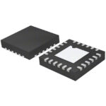 ADL5331ACPZ-R7

The activity of extra discounts on wholesale prices is in full swing…
Please fill in your contact information and we will send you the latest wholesale price list.






