 ChipApex | Global Electronic Components Supplier
SEARCH
Search Product
Search Post
— IC芯片 | 连接器 | 传感器 | 被动器件 —
Search productSearch post
— IC芯片 | 连接器 | 传感器 | 被动器件 —
Consult the customer manager about the wholesale price.
consultation hotline:86-132-6715-2157
email:[email protected]
Contact the product manager for consultation. One-stop consultation is available.
Do you want a lower wholesale price? Please send us your inquiry and we will reply immediately.
The ADM1181AANZ is a robust, high-speed, dual-channel RS-232/V.28 interface transceiver manufactured by Analog Devices Inc. It operates from a single 5 V power supply (4.5 V to 5.5 V) and supports data rates up to 230 kbps in full-duplex mode. The device integrates two drivers and two receivers with CMOS inputs and outputs. It features ±15 kV ESD protection on all I/O lines per the human body model and IEC1000-4-2 air discharge standards, along with ±2 kV electrical fast transient immunity. Internal circuitry includes a charge-pump voltage converter generating ±10 V rails using four external 0.1 µF capacitors. The component is housed in a 16-lead PDIP package and functions within an industrial temperature range of -40°C to +85°C.
Verify the specific ordering suffix 'ANZ' corresponds to the lead-free PDIP-16 package configuration as documented in the manufacturer's official datasheet. Confirm that the required external components, specifically four 0.1 µF capacitors for the charge pump, are included in the system design. Ensure the application environment remains within the specified industrial temperature limits and single 5 V supply constraints.
Select this component for applications requiring pin-compatible upgrades to legacy MAX202E or LT1181A designs where enhanced ruggedness is necessary. It is suitable for environments subject to frequent cable plugging or unplugging due to its superior transient protection capabilities. Consider the PDIP-16 package availability if surface-mount options like TSSOP are not required for the specific board layout constraints.
The ADM1181A belongs to the ADM202E/ADM1181A family of RS-232 line drivers and receivers. It serves as a direct replacement for older generation devices such as the LTC1181A. The series is designed to operate from a single 5 V supply while generating the higher voltages required for RS-232 signaling internally via charge-pump technology.
The ADM1181A is documented as a pin-compatible upgrade for the LTC1181A. Designers replacing legacy parts should verify that the existing PCB footprint accommodates the 16-lead PDIP package dimensions specified in the outline drawings.
Each receiver input contains an internal 5 kΩ pull-down resistor to ground. This ensures that unconnected inputs default to a Logic 1 output level, preventing floating signal states.
The device guarantees a maximum data rate of 230 kbps under worst-case loading conditions, supporting high-speed data links and ISDN modem standards.
No additional shielding or filtering is typically required. The device meets EN55022 and CISPR22 emission limits through internal design features like controlled slew rates and break-before-make switching in the charge pump.
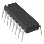 ADM1181AANZ
The activity of extra discounts on wholesale prices is in full swing…
Please fill in your contact information and we will send you the latest wholesale price list.





