 ChipApex | Global Electronic Components Supplier
ADN2819ACPZ-CML-RL
Search Product
Search Post
— IC芯片 | 连接器 | 传感器 | 被动器件 —
Search productSearch post
— IC芯片 | 连接器 | 传感器 | 被动器件 —
Consult the customer manager about the wholesale price.
consultation hotline:86-132-6715-2157
email:[email protected]
Contact the product manager for consultation. One-stop consultation is available.
Do you want a lower wholesale price? Please send us your inquiry and we will reply immediately.
The ADN2819ACPZ-CML-RL is a multirate clock and data recovery (CDR) integrated circuit from Analog Devices, designed for SONET/SDH and Gigabit Ethernet applications. It operates at data rates up to 2.7 GHz, supporting OC-3, OC-12, OC-48, GbE, and 15/14 FEC rates. The device features an integrated limiting amplifier with a typical quantizer sensitivity of 4 mV and adjustable slice levels. It meets stringent SONET jitter requirements for transfer, generation, and tolerance. Powered by a single 3.0 V to 3.6 V supply, it consumes approximately 540 mW. The component is housed in a compact 48-lead LFCSP package measuring 7 mm × 7 mm.
Verify the specific ordering suffix against the manufacturer's current documentation to confirm pinout compatibility and electrical characteristics. Ensure that the CML output configuration matches the system requirements, as other variants may offer different output types. Confirm availability through authorized distributors, as lead times may vary based on production status.
Select this component for high-speed optical receiver designs requiring integrated clock recovery and signal conditioning. The device supports both native rates and 15/14 rate digital wrappers without changing the reference clock frequency. Consider the power consumption of 540 mW and the thermal resistance of 25°C/W when designing the PCB layout. Ensure the reference clock source matches one of the supported frequencies: 19.44 MHz, 38.88 MHz, 77.76 MHz, or 155.52 MHz.
The ADN2819 belongs to Analog Devices' family of clock and data recovery ICs tailored for telecommunications infrastructure. It integrates functions typically found in separate components, such as a limiting amplifier, quantizer, and CDR loop, into a single chip. This integration reduces board space and simplifies design for fiber optic receivers when paired with a PIN diode and TIA preamplifier.
Publicly confirmed substitute part numbers are not available in the provided documentation. Evaluate alternative CDR devices from Analog Devices or other manufacturers based on pin compatibility, data rate support, and jitter performance specifications.
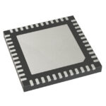 ADN2819ACPZ-CML-RL
The activity of extra discounts on wholesale prices is in full swing…
Please fill in your contact information and we will send you the latest wholesale price list.






