 ChipApex | Global Electronic Components Supplier
ADN2855ACPZ
Search Product
Search Post
— IC芯片 | 连接器 | 传感器 | 被动器件 —
Search productSearch post
— IC芯片 | 连接器 | 传感器 | 被动器件 —
Consult the customer manager about the wholesale price.
consultation hotline:86-132-6715-2157
email:[email protected]
Contact the product manager for consultation. One-stop consultation is available.
Do you want a lower wholesale price? Please send us your inquiry and we will reply immediately.
The ADN2855ACPZ is a burst mode clock and data recovery IC with an integrated deserializer, designed for GPON, BPON, and GEPON optical line terminal (OLT) receiver applications. It supports serial data rates of 155.52 Mbps, 622.08 Mbps, 1244.16 Mbps, and 1250.00 Mbps. The device features a patented dual-loop architecture that frequency locks to an OLT reference clock and acquires phase lock within 12 bits of the preamble start. It provides a 4-bit parallel LVDS output interface or a serial output option, along with a byte rate reference clock compatible with double data rate (DDR) FPGAs. Operating on a single 3.3 V supply, it consumes 670 mW in serial mode and 825 mW in deserializer mode.
Verify the specific package marking and date code against the manufacturer's ordering guide to ensure compliance with the CP-32-20 outline dimensions updated in Revision B. Confirm that the application design accounts for the required 0.47 µF ± 20% X7R ceramic capacitor on the frequency loop pins (CF1/CF2) with low leakage characteristics to maintain jitter specifications.
Select this component when designing OLT receivers requiring burst-mode operation with strict acquisition time constraints. Ensure the system provides a stable reference clock between 10 MHz and 200 MHz for the FLL. Verify FPGA compatibility with the available DDR clock modes if high-speed parallel processing is required. Note that the device requires a RESET pulse between bursts to reset the acquisition state.
The ADN2855 belongs to Analog Devices' specialized timing portfolio for passive optical networks. Unlike continuous-rate CDRs, it is optimized for the bursty traffic patterns inherent in PON upstream transmissions. It integrates a PRBS generator for testing and supports I2C control for dynamic rate switching without external programming hardware during normal operation.
Public confirmed substitute part numbers are not available in the provided documentation. Designers should consult Analog Devices for current alternatives within the ADN28xx series or newer generations of PON receiver solutions.
The device uses a preamble detector to identify the maximum transition density pattern (1010...) in the preamble. Once detected, the D/PLL acquires phase lock within 12 UI of this pattern start, following a RESET assertion.
The REFCLK input provides a frequency reference locked to the incoming data. The ADN2855 uses its FLL to acquire frequency lock relative to this reference clock before performing phase acquisition on the data burst.
No, the ADN2855 is designed specifically for burst mode recovery which requires a reference clock for frequency acquisition. It must be operated in 'lock to reference clock' mode by setting CTRLA Bit 0 to 1.
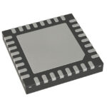 ADN2855ACPZ
The activity of extra discounts on wholesale prices is in full swing…
Please fill in your contact information and we will send you the latest wholesale price list.






