 ChipApex | Global Electronic Components Supplier
SEARCH
Search Product
Search Post
— IC芯片 | 连接器 | 传感器 | 被动器件 —
Search productSearch post
— IC芯片 | 连接器 | 传感器 | 被动器件 —
Consult the customer manager about the wholesale price.
consultation hotline:86-132-6715-2157
email:[email protected]
Contact the product manager for consultation. One-stop consultation is available.
Do you want a lower wholesale price? Please send us your inquiry and we will reply immediately.
The AFS090-1FGG256 is a Fusion mixed signal FPGA featuring 90,000 system gates and 2,304 tiles. It utilizes an advanced 130-nm flash-based CMOS process with seven layers of metal. The device includes 2 Mbits of user flash memory and 1 Kbit of FlashROM. Integrated analog resources comprise a 12-bit ADC supporting up to 30 channels at 600 Ksps and five Analog Quads with gate driver outputs. Clocking is provided by six Clock Conditioning Circuits (CCCs) with one integrated PLL. The FG256 package offers 75 single-ended or 22 differential I/Os. It operates from a single 3.3 V supply with an on-chip 1.5 V regulator.
Verify the specific ordering suffix against the manufacturer's current product status documentation. Confirm that the requested package variant matches the required pin count and thermal specifications. Ensure the selected speed grade aligns with the target system timing requirements before finalizing procurement orders.
Select this component when a single-chip solution combining digital logic with analog power control is required. The AFS090 density suits designs needing moderate logic capacity alongside significant analog integration. Consider the FG256 package constraints regarding available I/O banks and routing resources for complex mixed-signal layouts.
This part belongs to the Microsemi Fusion family of mixed signal FPGAs. It shares architectural similarities with higher-density models like the AFS250 and AFS600 but offers reduced logic capacity. The device is designed as a cost-effective alternative to discrete analog components and ASICs for system management tasks.
Devices within the same package type across the Fusion family, such as the AFS250, may offer pin compatibility. Verify electrical characteristics and resource availability when substituting with other members of the ProASIC3 or SmartFusion families.
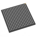 AFS090-1FGG256
The activity of extra discounts on wholesale prices is in full swing…
Please fill in your contact information and we will send you the latest wholesale price list.





