 ChipApex | Global Electronic Components Supplier

SEARCH
Search Product
Search Post
— IC芯片 | 连接器 | 传感器 | 被动器件 —
Search productSearch post
— IC芯片 | 连接器 | 传感器 | 被动器件 —
Consult the customer manager about the wholesale price.
consultation hotline:86-132-6715-2157
email:[email protected]
Contact the product manager for consultation. One-stop consultation is available.
Do you want a lower wholesale price? Please send us your inquiry and we will reply immediately.
The AO6415 is a P-Channel Enhancement Mode Field Effect Transistor manufactured by Alpha & Omega Semiconductor Inc. It utilizes advanced trench technology to deliver low on-resistance and gate charge, supporting operation with gate voltages as low as 2.5V. The device features a Drain-Source Voltage (VDS) of -20V and a continuous Drain Current (ID) of -3.3A at VGS=-10V. On-resistance (RDS(ON)) is specified as less than 82mΩ at VGS=-10V, less than 100mΩ at VGS=-4.5V, and less than 140mΩ at VGS=-2.5V. It is housed in a TSOP6 package.
Verify the specific ordering suffix against the manufacturer's official documentation to confirm environmental compliance status, such as RoHS or lead-free specifications. Ensure that the procurement channel sources components directly from authorized distributors to guarantee authenticity and traceability. Cross-reference the part number with the latest datasheet revision to confirm electrical characteristics match the intended design requirements before finalizing orders.
Select this component for circuits requiring a compact P-Channel MOSFET with a 20V voltage rating. Consider the thermal resistance values when designing heat dissipation strategies, as junction-to-ambient impedance varies based on board copper area and airflow conditions. Evaluate the gate threshold voltage range to ensure reliable turn-on and turn-off behavior within the target system's control voltage levels.
This component belongs to the Alpha & Omega Semiconductor lineup of power management discrete semiconductors. It is designed for general-purpose switching tasks where space constraints and efficiency are priorities. The TSOP6 package allows for surface-mount integration into dense printed circuit board layouts common in portable electronics and computing peripherals.
When evaluating substitutes, verify that the alternative device maintains a compatible Drain-Source Voltage of at least -20V and a continuous current rating equal to or exceeding -3.3A. Ensure the replacement offers similar RDS(ON) characteristics at the operating gate voltage to maintain equivalent power loss profiles.
The absolute maximum Gate-Source Voltage (VGS) rating is ±12V.
Yes, the device includes an internal body diode with a continuous current rating of -1.5A and a reverse recovery time of 6.1ns.
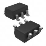 AO6415

The activity of extra discounts on wholesale prices is in full swing…
Please fill in your contact information and we will send you the latest wholesale price list.





