 ChipApex | Global Electronic Components Supplier
SEARCH
Search Product
Search Post
— IC芯片 | 连接器 | 传感器 | 被动器件 —
Search productSearch post
— IC芯片 | 连接器 | 传感器 | 被动器件 —
Consult the customer manager about the wholesale price.
consultation hotline:86-132-6715-2157
email:[email protected]
Contact the product manager for consultation. One-stop consultation is available.
Do you want a lower wholesale price? Please send us your inquiry and we will reply immediately.
The AO6802 is a dual N-channel MOSFET manufactured by Alpha & Omega Semiconductor. It features a maximum drain-source voltage of 30V and a continuous drain current of 3.5A at VGS=10V. The device utilizes advanced trench technology to achieve low on-resistance, specified as less than 50mΩ at VGS=10V and less than 70mΩ at VGS=4.5V. Key electrical parameters include a gate threshold voltage ranging from 1.5V to 2.5V, total gate charge of 4.05nC at 10V, and input capacitance of 210pF. The component operates within a junction temperature range of -55°C to 150°C and is housed in a TSOP-6 surface-mount package.
Verify the specific datasheet revision against the manufacturer's official documentation before finalizing design specifications. Confirm that the TSOP-6 package dimensions align with the target PCB footprint. Ensure thermal management strategies account for the junction-to-ambient resistance values provided in the static characteristics section of the data sheet.
Select this component when a compact dual N-channel solution is required for 30V logic-level switching. The low gate charge facilitates faster switching speeds with minimal driver current requirements. Evaluate the on-resistance performance at the intended operating gate voltage to ensure efficiency meets system constraints under expected load conditions.
The AO6802 belongs to the Alpha & Omega Semiconductor family of dual MOSFET arrays designed for space-constrained designs. It serves as an alternative to discrete single-channel implementations where board area is limited. The device integrates two identical N-channel FETs into a single six-terminal package to simplify assembly and reduce overall component count.
Direct pin-compatible replacements must maintain the 30V rating, TSOP-6 package, and comparable RDS(ON) thresholds. Verify that any substitute part supports the same logic-level gate drive voltages and thermal dissipation characteristics to ensure circuit compatibility without redesign.
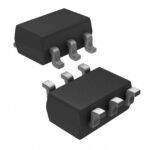 AO6802
The activity of extra discounts on wholesale prices is in full swing…
Please fill in your contact information and we will send you the latest wholesale price list.





