 ChipApex | Global Electronic Components Supplier
SEARCH
Search Product
Search Post
— IC芯片 | 连接器 | 传感器 | 被动器件 —
Search productSearch post
— IC芯片 | 连接器 | 传感器 | 被动器件 —
Consult the customer manager about the wholesale price.
consultation hotline:86-132-6715-2157
email:[email protected]
Contact the product manager for consultation. One-stop consultation is available.
Do you want a lower wholesale price? Please send us your inquiry and we will reply immediately.
The ALD1101SAL is a monolithic dual N-channel matched MOSFET pair manufactured using enhanced ACMOS silicon gate CMOS process. It features an 8-pin SOIC surface-mount package with a drain-source voltage rating of 10V and power dissipation of 500mW. The device operates within a temperature range of 0°C to +70°C. Key electrical parameters include a gate threshold voltage (VT) of 0.4V to 1.0V, offset voltage (VOS) of 2mV to 10mV, on-resistance (RDS(ON)) of 50Ω to 75Ω at VGS=5V, and input capacitance (CISS) of 6pF to 10pF.
Verify the specific grade suffix (A, B, or unmarked) required for your application's offset voltage tolerance before ordering. Confirm that the 8-SOIC package dimensions align with your PCB footprint design. Ensure static control procedures are followed during handling due to ESD sensitivity.
Select the ALD1101ASAL for tighter offset voltage specifications (2mV max), ALD1101BSAL for moderate specs (5mV max), or ALD1101SAL for standard specifications (10mV max). Consider the ALD1102 companion device if constructing complementary CMOS analog switches. Verify operating voltage requirements against the 10V maximum rating.
The ALD1101 belongs to the ALD1101/ALD1102 family of precision matched MOSFET pairs from Advanced Linear Devices. These devices utilize ACMOS technology to provide high input impedance and low leakage, distinguishing them from standard discrete transistors in analog signal processing roles.
No direct public substitute part numbers are documented for this specific component.
The typical input impedance is 10^12 Ω.
The ALD1101 is a dual N-channel matched pair, while the ALD1102 is a dual P-channel matched pair. They are often used together to construct CMOS analog switches.
The absolute maximum gate-source voltage (VGS) is 10V.
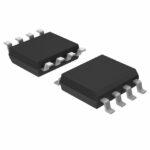 ALD1101SAL
The activity of extra discounts on wholesale prices is in full swing…
Please fill in your contact information and we will send you the latest wholesale price list.





