 ChipApex | Global Electronic Components Supplier
SEARCH
Search Product
Search Post
— IC芯片 | 连接器 | 传感器 | 被动器件 —
Search productSearch post
— IC芯片 | 连接器 | 传感器 | 被动器件 —
Consult the customer manager about the wholesale price.
consultation hotline:86-132-6715-2157
email:[email protected]
Contact the product manager for consultation. One-stop consultation is available.
Do you want a lower wholesale price? Please send us your inquiry and we will reply immediately.
The AOB2606L is a surface-mount N-channel MOSFET from Alpha & Omega Semiconductor, utilizing Trench technology for optimized high-frequency switching. It features a drain-source voltage (VDS) of 60V and a continuous drain current (ID) of 72A at VGS=10V. The device exhibits an extremely low on-state resistance (RDS(ON)) of less than 6.5mW at VGS=10V and ID=20A. Key electrical parameters include a gate threshold voltage (VGS(th)) ranging from 2.5V to 3.5V, total gate charge (Qg) of 53nC to 75nC at 10V, and input capacitance (Ciss) of 4050pF. It supports a maximum junction temperature of 175°C and has been subjected to 100% UIS and Rg testing.
Verify the specific package variant required, as the datasheet covers TO-263 (D2PAK), TO-220, and TO-220F packages under the same part number family. Confirm that the application environment respects the absolute maximum ratings, particularly the 175°C junction temperature limit and thermal impedance constraints. Ensure compatibility with the specified gate drive voltages for optimal RDS(ON) performance.
Select this component for applications requiring high efficiency in high-frequency switching environments due to its minimized switching losses. Consider the thermal management requirements carefully, as the junction-to-ambient thermal resistance varies significantly by package type. Verify that the 60V rating provides sufficient headroom for the specific circuit's peak voltage transients.
The AOB2606L belongs to the AOT2606L/AOB2606L/AOTF2606L series of 60V N-Channel MOSFETs manufactured by Alpha & Omega Semiconductor. These devices are designed using Trench MOSFET technology to deliver efficient high-frequency switching performance. The series is characterized by low on-resistance and capacitance, making it suitable for various power supply topologies.
Direct substitutes within the same series include AOT2606L (TO-220 package) and AOTF2606L (TO-220F package). When replacing, verify that the physical footprint and pinout of the new package match the existing PCB design, as thermal characteristics differ between surface mount and through-hole variants.
The maximum junction temperature (TJ) for the AOB2606L is 175°C.
Yes, the device undergoes 100% Unclamped Inductive Switching (UIS) testing.
The total gate charge (Qg) at VGS=10V ranges from 53nC to 75nC.
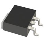 AOB2606L
The activity of extra discounts on wholesale prices is in full swing…
Please fill in your contact information and we will send you the latest wholesale price list.





