 ChipApex | Global Electronic Components Supplier

SEARCH
Search Product
Search Post
— IC芯片 | 连接器 | 传感器 | 被动器件 —
Search productSearch post
— IC芯片 | 连接器 | 传感器 | 被动器件 —
Consult the customer manager about the wholesale price.
consultation hotline:86-132-6715-2157
email:[email protected]
Contact the product manager for consultation. One-stop consultation is available.
Do you want a lower wholesale price? Please send us your inquiry and we will reply immediately.
The AOD3N80 is an N-channel MOSFET fabricated using an advanced high-voltage process, rated for a drain-source voltage of 800V and a continuous drain current of 2.8A at 25°C. It features a maximum on-resistance of less than 4.8W at VGS=10V and supports a peak diode recovery dv/dt of 5V/ns. The device includes guaranteed avalanche capability with repetitive energy ratings up to 72mJ and single-pulse ratings up to 145mJ. Thermal characteristics include a junction-to-case resistance of 1.5°C/W and a junction-to-ambient resistance of 55°C/W.
Verify the specific datasheet revision against the manufacturer's official documentation before finalizing design specifications. Confirm that the TO252 package dimensions align with the target PCB footprint requirements. Ensure thermal management strategies account for the specified junction-to-ambient and junction-to-case thermal resistances under intended operating conditions.
Select this component for applications requiring high voltage blocking capabilities combined with moderate current handling in compact surface-mount packages. Consider the guaranteed avalanche rating when designing circuits subject to inductive load switching or transient voltage spikes. Evaluate the gate charge parameters to ensure compatibility with available driver circuitry for optimal switching performance.
This part belongs to the Alpha & Omega Semiconductor lineup of high-voltage discrete semiconductors designed for power conversion. It utilizes the company's proprietary high-voltage MOSFET technology to balance conduction losses with switching speed. The TO252 (DPAK) package provides a cost-effective solution for medium-power applications where board space is limited but thermal dissipation remains a critical design factor.
No public confirmed substitute part numbers are documented in the provided source material.
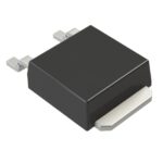 AOD3N80

The activity of extra discounts on wholesale prices is in full swing…
Please fill in your contact information and we will send you the latest wholesale price list.





