ChipApex | Global Electronic Components Supplier
SEARCH
Search Product
Search Post
— IC芯片 | 连接器 | 传感器 | 被动器件 —
Search productSearch post
— IC芯片 | 连接器 | 传感器 | 被动器件 —
Consult the customer manager about the wholesale price.
consultation hotline:86-132-6715-2157
email:[email protected]
Contact the product manager for consultation. One-stop consultation is available.
Do you want a lower wholesale price? Please send us your inquiry and we will reply immediately.
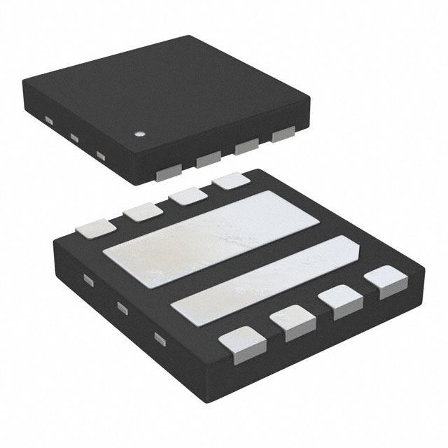
The AON7932 is a dual asymmetric N-channel MOSFET in a Power DFN3x3A package. It integrates two specialized transistors for synchronous buck converters. Q1 (High Side) features low gate charge to minimize switching losses, while Q2 (Low Side) utilizes advanced trench technology with an integrated Schottky diode for low RDS(ON). The device supports a drain-source voltage of 30V. Q1 offers a maximum on-resistance of <20mΩ at VGS=10V and <30mΩ at VGS=4.5V. Q2 provides <12mΩ at VGS=10V and <15mΩ at VGS=4.5V. Both channels are 100% UIS tested.
Verify the component against the official Alpha & Omega Semiconductor datasheet Rev.3.0. Confirm the package type is Power DFN3x3A and check for specific ordering suffixes if required by the design. Ensure the source documentation matches the manufacturer's part identification exactly.
Select this component for space-constrained synchronous buck converters requiring optimized thermal performance. The asymmetric design allows independent optimization of switching and conduction losses. Verify that the 30V rating and current capabilities meet the specific circuit requirements.
This component belongs to the Alpha & Omega Semiconductor dual MOSFET family. It is specifically designed to replace discrete high-side and low-side MOSFET solutions in synchronous rectification topologies, offering improved board space utilization and electrical performance.
Public confirmed substitute part numbers are not available in the provided documentation. Consult the manufacturer's cross-reference tools or updated product lists for potential replacements.
The maximum Drain-Source Voltage (BVDSS) is 30V.
The Q2 channel uses advanced trench technology with a monolithically integrated Schottky diode to provide excellent RDS(ON), whereas the Q1 channel is designed to minimize switching losses.
Yes, both channels are 100% UIS tested.
 AON7932_101
The activity of extra discounts on wholesale prices is in full swing…
Please fill in your contact information and we will send you the latest wholesale price list.