 ChipApex | Global Electronic Components Supplier
SEARCH
Search Product
Search Post
— IC芯片 | 连接器 | 传感器 | 被动器件 —
Search productSearch post
— IC芯片 | 连接器 | 传感器 | 被动器件 —
Consult the customer manager about the wholesale price.
consultation hotline:86-132-6715-2157
email:[email protected]
Contact the product manager for consultation. One-stop consultation is available.
Do you want a lower wholesale price? Please send us your inquiry and we will reply immediately.
The AOTS26108 is a complementary MOSFET array featuring an N-channel and P-channel pair in a single TSOP-6 package. The N-channel device provides a drain-source voltage (VDS) of 30V with a continuous drain current (ID) of 3.8A at VGS=10V, while the P-channel offers -20V VDS and -4.5A ID at VGS=-4.5V. On-resistance for the N-channel is less than 50mΩ at VGS=10V and 57mΩ at VGS=4.5V. The P-channel on-resistance is under 44mΩ at VGS=-4.5V and 59mΩ at VGS=-2.5V. Total gate charge is 16nC at 10V for the N-channel and 17nC at 4.5V for the P-channel. The component operates within a junction temperature range of -55°C to 150°C.
Verify the specific ordering suffix against the manufacturer's official documentation to confirm exact packaging and compliance status. Confirm that the intended application does not involve life support systems, as such usage is explicitly unauthorized by Alpha & Omega Semiconductor. Ensure thermal management aligns with the specified junction-to-ambient resistance values provided in the datasheet.
Select this component when space constraints require a matched complementary pair in a small outline package. Evaluate the gate threshold voltage requirements against the available drive voltage levels, noting the distinct performance metrics at 10V versus lower logic-level voltages. Consider the thermal characteristics relative to the expected duty cycle and ambient conditions.
Alpha & Omega Semiconductor manufactures the AOTS26108 utilizing Trench Power MOSFET technology. This product line targets applications requiring efficient power switching in compact form factors. The company specializes in discrete power devices and power management solutions for consumer electronics and industrial equipment.
No verified public substitute part numbers are documented for the AOTS26108.
The maximum gate-source voltage is ±12V for the N-channel and ±8V for the P-channel.
For the N-channel, RDS(ON) increases from less than 50mΩ at VGS=10V to less than 72mΩ at VGS=2.5V. For the P-channel, it rises from less than 44mΩ at VGS=-4.5V to less than 80mΩ at VGS=-1.8V.
The typical body diode reverse recovery time (trr) is 5.5ns for the N-channel and 25ns for the P-channel.
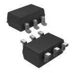 AOTS26108
The activity of extra discounts on wholesale prices is in full swing…
Please fill in your contact information and we will send you the latest wholesale price list.





