 ChipApex | Global Electronic Components Supplier
SEARCH
Search Product
Search Post
— IC芯片 | 连接器 | 传感器 | 被动器件 —
Search productSearch post
— IC芯片 | 连接器 | 传感器 | 被动器件 —
Consult the customer manager about the wholesale price.
consultation hotline:86-132-6715-2157
email:[email protected]
Contact the product manager for consultation. One-stop consultation is available.
Do you want a lower wholesale price? Please send us your inquiry and we will reply immediately.
The ALD1103PBL is a monolithic dual N-channel and dual P-channel matched MOSFET pair housed in a 14-pin Plastic DIP package. It features a low threshold voltage of 0.7V, low input capacitance of 610pF, and an offset voltage of 10mV. The device operates within a +2V to +10V supply range with a maximum drain-source voltage of 10V. Thermal tracking between pairs ensures minimal differential thermal response, while high input impedance and negative current temperature coefficient support precision analog applications.
Verify the specific ordering suffix against manufacturer documentation to confirm package type and compliance status. Confirm that the component meets RoHS requirements if applicable to the design. Ensure static control procedures are utilized during handling due to ESD sensitivity. Validate operating temperature ranges align with system specifications before procurement.
Select this component for applications requiring high input impedance and low offset voltage in low-voltage systems. Consider the 10V absolute maximum ratings when designing power supplies. Evaluate the negative current temperature coefficient for thermal stability requirements. Ensure the chosen package variant matches the PCB layout constraints.
The ALD1103 belongs to a family of matched MOSFET pairs manufactured using ACMOS silicon gate CMOS process. It combines the functions of the ALD1101 N-channel pair and ALD1102 P-channel pair into a single package. This integration facilitates compact designs for analog signal processing and switching applications.
Direct replacements include the ALD1101SBL or ALD1102SBL if only one channel type is required. Verify pin compatibility and electrical characteristics such as threshold voltage and on-resistance when substituting with other matched MOSFET pairs from different manufacturers.
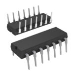 ALD1103PBL
The activity of extra discounts on wholesale prices is in full swing…
Please fill in your contact information and we will send you the latest wholesale price list.





