 ChipApex | Global Electronic Components Supplier
ASNT8050-PQB
Search Product
Search Post
— IC芯片 | 连接器 | 传感器 | 被动器件 —
Search productSearch post
— IC芯片 | 连接器 | 传感器 | 被动器件 —
Consult the customer manager about the wholesale price.
consultation hotline:86-132-6715-2157
email:[email protected]
Contact the product manager for consultation. One-stop consultation is available.
Do you want a lower wholesale price? Please send us your inquiry and we will reply immediately.
The ASNT8050-PQB is a programmable Phase-Locked Loop (PLL) with integrated Voltage-Controlled Oscillators (VCOs), fabricated in SiGe technology. It operates as a clock multiplication unit (CMU) or divider, supporting two selectable frequency ranges: 7.4–8.8 GHz and 10.8–12.7 GHz. The device accepts LVDS or CML reference inputs and provides full-rate CML outputs and LVDS divided outputs. Key electrical parameters include a single +3.3V supply, 630 mW power consumption, and closed-loop SSB phase noise better than -98 dBc/Hz at a 10 MHz offset. It features an external RC loop filter interface and a 40-pin MLF/QFN package.
Verify the specific revision level against the manufacturer's documentation, as updates may affect pinout or electrical characteristics. Confirm that the external loop filter components match the recommended schematic for the desired bandwidth and phase margin. Ensure the PCB layout accommodates the 40-pin QFN package thermal requirements by soldering the center heat slug to the ground plane.
Select this component when dual-frequency coverage (X-band and Ku-band ranges) is required from a single IC. Choose based on the need for flexible input interfaces (LVDS/CML) and the ability to operate in open-loop VCO control mode if external voltage tuning is necessary. Consider the 630 mW power dissipation and ensure adequate thermal management for the QFN package within the operating temperature range of -40°C to 125°C junction temperature.
The ASNT8050 series belongs to Advanced Science And Novel Technology Company's portfolio of high-performance RF timing devices. The 'PQB' suffix denotes the specific 40-pin MLF/QFN package variant. This family utilizes SiGe BiCMOS technology to achieve high linearity and low phase noise, distinguishing it from standard CMOS PLLs which may struggle at these high frequencies.
No direct public substitutes are listed in the provided datasheet. Cross-referencing requires matching the dual-VCO architecture, SiGe fabrication process, and specific frequency ranges. Devices from other manufacturers typically require separate VCOs and PLL chips to replicate this integration level.
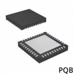 ASNT8050-PQB
The activity of extra discounts on wholesale prices is in full swing…
Please fill in your contact information and we will send you the latest wholesale price list.






