 ChipApex | Global Electronic Components Supplier
SEARCH
Search Product
Search Post
— IC芯片 | 连接器 | 传感器 | 被动器件 —
Search productSearch post
— IC芯片 | 连接器 | 传感器 | 被动器件 —
Consult the customer manager about the wholesale price.
consultation hotline:86-132-6715-2157
email:[email protected]
Contact the product manager for consultation. One-stop consultation is available.
Do you want a lower wholesale price? Please send us your inquiry and we will reply immediately.
The AT17F080-30TQC is an 8-Mbit serial configuration memory device designed for Field Programmable Gate Arrays (FPGAs). It operates at a maximum clock frequency of 33 MHz and supports In-System Programming via a 2-wire bus. The component utilizes a low-power CMOS Flash process with 5V tolerant I/O pins and a 3.3V output capability. It is housed in a 44-lead Thin Plastic Quad Flat Package (TQFP) and functions within a commercial temperature range of 0°C to +70°C.
Verify the specific package suffix TQFP corresponds to the 44-lead Thin Quad Flat Package variant. Confirm the operating temperature grade matches the commercial requirement of 0°C to +70°C. Ensure programming equipment supports the required 2-wire serial protocol for ISP operations. Check for compatibility with the intended FPGA master serial mode signals.
Select this component when an 8-Mbit capacity is required for FPGA configuration. Choose this part over the AT17F040 if the target design exceeds 4-Mbit storage needs. Consider the TQFP package only if surface mount assembly on a 44-pin footprint is available. Verify that the system voltage aligns with the 3.3V nominal supply specification.
This device belongs to the AT17F Series of In-System Programmable Configuration PROMs. These configurators provide cost-effective memory solutions for SRAM-based FPGAs. The series includes variants like the AT17F040 for smaller designs. The AT17F080 specifically targets applications requiring larger configuration data sets.
AT17F080-30BJC (44-lead PLCC package)
The CEO pin goes Low when the internal address counter reaches its maximum value, enabling the CE input of the next device in the chain to drive its DATA output.
When high, it partitions the address space into four equal pages, allowing multiple configuration bitstreams to be stored and retrieved from a single device using PAGESEL inputs.
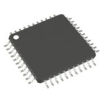 AT17F080-30TQC
The activity of extra discounts on wholesale prices is in full swing…
Please fill in your contact information and we will send you the latest wholesale price list.





