 ChipApex | Global Electronic Components Supplier
SEARCH
Search Product
Search Post
— IC芯片 | 连接器 | 传感器 | 被动器件 —
Search productSearch post
— IC芯片 | 连接器 | 传感器 | 被动器件 —
Consult the customer manager about the wholesale price.
consultation hotline:86-132-6715-2157
email:[email protected]
Contact the product manager for consultation. One-stop consultation is available.
Do you want a lower wholesale price? Please send us your inquiry and we will reply immediately.
The AT94K40AL-25DQU is a monolithic Field Programmable System Level Integrated Circuit (FPSLIC) combining an Atmel AT40K SRAM-based FPGA with an embedded high-performance AVR RISC microcontroller core. The device features 40,000 usable FPGA gates and up to 36 Kbytes of dynamically allocated instruction and data SRAM. It operates at a maximum frequency of 25 MHz within a voltage range of 3.0V to 3.6V. Key specifications include a hardware multiplier, JTAG ICE support, two UARTs, and multiple timer/counters.
Verify the ordering suffix 'DQU' corresponds to the specific package type and temperature grade defined in the official datasheet. Confirm that the 'J' designation for JTAG ICE support is present in the date code or part marking if debug capabilities are required. Ensure PCB layout supports split power supplies as recommended for the AT94KAL series.
Select this model when 40,000 FPGA gates and extensive SRAM resources are necessary for complex mixed-signal designs. The 25MHz speed grade suits applications where moderate processing speed is sufficient. Consider the AT94K10AL or AT94K05AL variants if gate counts and memory requirements are lower to optimize cost and pin count.
This component belongs to the AT94KAL Series FPSLIC family, which integrates SRAM FPGAs with AVR microcontrollers. It shares architectural similarities with the AT94SAL series but utilizes SRAM-based technology rather than flash. The device is fabricated using a 0.35µm five-layer metal CMOS process.
Direct replacements within the same package and performance tier include other members of the AT94KAL series, such as the AT94K10AL or AT94K05AL, provided the gate count and memory requirements align with the application design.
The AT40K FPGA core supports Cache Logic, allowing partial or full logic reconfiguration without loss of data. The AVR core can reprogram the FPGA during operation to load new logic functions while maintaining active data.
JTAG ICE (In-Circuit Emulator) support provides extensive on-chip debug capabilities compliant with IEEE std. 1149.1. It allows for boundary-scan testing and detailed debugging of the AVR ports and system logic.
Up to 36 Kbytes of 15 ns dual-port SRAM is shared. The AVR accesses one side for program instructions and data, while the FPGA accesses the other side for data storage without consuming AVR bus bandwidth. Memory partitions can be configured during development.
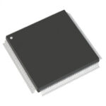 AT94K40AL-25DQU
The activity of extra discounts on wholesale prices is in full swing…
Please fill in your contact information and we will send you the latest wholesale price list.





