 ChipApex | Global Electronic Components Supplier
SEARCH
Search Product
Search Post
— IC芯片 | 连接器 | 传感器 | 被动器件 —
Search productSearch post
— IC芯片 | 连接器 | 传感器 | 被动器件 —
Consult the customer manager about the wholesale price.
consultation hotline:86-132-6715-2157
email:[email protected]
Contact the product manager for consultation. One-stop consultation is available.
Do you want a lower wholesale price? Please send us your inquiry and we will reply immediately.
The ATF1502ASV-15AC44 is a high-performance, high-density complex programmable logic device (CPLD) utilizing electrically-erasable technology. It features 32 macrocells with up to 36 inputs and operates within a 3.0V to 3.6V supply range. The device offers a maximum pin-to-pin delay of 15 ns and supports registered operation up to 77 MHz. It includes enhanced routing resources, in-system programmability via JTAG, and advanced power management features such as pin-controlled standby mode.
Verify the package type matches the required application, as the ATF1502ASV series is available in both 44-lead PLCC and TQFP configurations. Confirm that the commercial temperature range (0°C to 70°C) meets system requirements, or select the industrial variant if wider temperature tolerance is necessary. Ensure programming tools support the IEEE 1149.1 JTAG standard for in-system configuration.
Select this component when 32 macrocells are sufficient for the design complexity. The -15 suffix indicates a 15 ns maximum delay, suitable for applications requiring up to 100 MHz clock frequencies. Consider the enhanced routing resources if the design requires significant pin-locking constraints. Verify that the 3.3V operating voltage aligns with the rest of the system's I/O levels.
This part belongs to the ATF1502ASV family of CPLDs manufactured by Microchip Technology (formerly Atmel). The 'AC' suffix denotes the commercial temperature grade and 15 ns speed class. It is designed to replace older discrete logic and simple PLDs, offering higher density and reprogrammability through EEPROM technology.
For industrial temperature requirements, consider the ATF1502ASV-15JI44. For lower speed requirements, the ATF1502ASV-20AC44 is available. Direct replacements must maintain the 44-pin footprint and 3.3V operation unless level shifting is implemented.
Each macrocell has 5 product terms, which can be expanded up to 40 product terms using the cascade logic feature.
The ATF1502ASV offers a programmable pin-keeper option that holds floating input and I/O pins at their previous state, preventing unnecessary power consumption and system noise without external pull-up resistors.
Yes, if JTAG boundary-scan testing or in-system programming is not required, the four JTAG control pins (TDI, TMS, TCK, TDO) can be configured as general-purpose I/O pins.
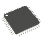 ATF1502ASV-15AC44
The activity of extra discounts on wholesale prices is in full swing…
Please fill in your contact information and we will send you the latest wholesale price list.





