 ChipApex | Global Electronic Components Supplier
SEARCH
Search Product
Search Post
— IC芯片 | 连接器 | 传感器 | 被动器件 —
Search productSearch post
— IC芯片 | 连接器 | 传感器 | 被动器件 —
Consult the customer manager about the wholesale price.
consultation hotline:86-132-6715-2157
email:[email protected]
Contact the product manager for consultation. One-stop consultation is available.
Do you want a lower wholesale price? Please send us your inquiry and we will reply immediately.
The BCM856SE6327BTSA1 is a PNP silicon AF transistor array featuring two galvanically isolated transistors in an SOT363 package. It provides a collector-emitter voltage (VCEO) of 65 V and a maximum collector current (IC) of 100 mA, with a peak current capability of 200 mA for pulses under 10 ms. The device offers a transition frequency (fT) of 250 MHz at IC = 20 mA and VCE = 5 V. DC current gain ranges from 200 to 450 depending on the operating point. Total power dissipation is rated at 250 mW at a case temperature of 115 °C.
Verify the specific ordering suffix E6327BTSA1 against official Infineon documentation to confirm tape-and-reel specifications and marking details. Ensure compatibility with AEC Q101 qualification requirements if automotive deployment is intended. Cross-reference the exact part number with authorized distributors to validate availability and authenticity before procurement.
Select this component when a compact dual PNP configuration with high precision matching is required. The low saturation voltage makes it suitable for efficient switching or amplification stages where minimal voltage drop is critical. Consider the thermal resistance characteristics and total power dissipation limits during circuit design to ensure reliable operation within the specified junction temperature range.
This part belongs to the BCM856S family of PNP silicon AF transistor arrays. It serves as the complementary counterpart to the BCM846S NPN array. The series is designed for general-purpose analog and RF applications requiring small signal processing capabilities in a space-saving surface-mount package.
The BC856S is listed as a reference part for orientation purposes. Verify electrical parameter equivalence and pinout compatibility before substitution. No other direct substitutes are confirmed in the provided documentation.
The maximum collector-emitter breakdown voltage (V(BR)CEO) is 65 V when IC = 10 mA and IB = 0 A.
Matching is defined by the difference in collector currents (∆IC), which is specified to be within ±10% at IB = 1 µA and IB = 100 µA with VCE1 = VCE2 = 1.0 V.
The transition frequency (fT) is typically 250 MHz, measured at IC = 20 mA, VCE = 5 V, and f = 100 MHz.
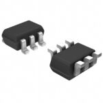 BCM856SE6327BTSA1
The activity of extra discounts on wholesale prices is in full swing…
Please fill in your contact information and we will send you the latest wholesale price list.





