ChipApex | Global Electronic Components Supplier
SEARCH
Search Product
Search Post
— IC芯片 | 连接器 | 传感器 | 被动器件 —
Search productSearch post
— IC芯片 | 连接器 | 传感器 | 被动器件 —
Consult the customer manager about the wholesale price.
consultation hotline:86-132-6715-2157
email:[email protected]
Contact the product manager for consultation. One-stop consultation is available.
Do you want a lower wholesale price? Please send us your inquiry and we will reply immediately.
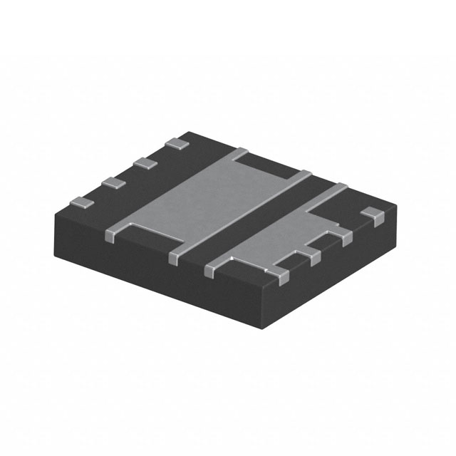
The BSC0910NDI is a dual N-channel OptiMOS™ MOSFET in a PG-TISON-8 package. It features a 25 V drain-source breakdown voltage and logic-level gate drive rated at 4.5 V. Maximum on-state resistance is 5.9 mΩ at 10 V gate drive for Q1, and 1.6 mΩ for Q2. Continuous drain current reaches 40 A at Tc=70°C. The device includes an integrated monolithic Schottky-like diode and is qualified according to JEDEC standards.
Verify the component against the official Infineon datasheet revision 2.0. Confirm the specific marking code '0910NDI' matches the PG-TISON-8 package footprint. Ensure that the ordering suffix corresponds to the required tape and reel quantity specifications defined by the manufacturer.
Select this component for low-voltage synchronous rectification where compact packaging is required. Evaluate thermal resistance values relative to the PCB copper area. Consider the asymmetric RDS(on) characteristics between the two channels when designing the control loop.
This part belongs to the OptiMOS™ family of power MOSFETs designed for efficiency and reliability. It utilizes silicon technology within a surface-mount package suitable for automated assembly processes in consumer and industrial electronics manufacturing.
Check pinout compatibility with existing PG-TISON-8 footprints. Verify that alternative devices meet the 25 V breakdown voltage requirement and support the necessary 4.5 V logic-level gate drive threshold.
 BSC0910NDIATMA1
The activity of extra discounts on wholesale prices is in full swing…
Please fill in your contact information and we will send you the latest wholesale price list.