 ChipApex | Global Electronic Components Supplier

SEARCH
Search Product
Search Post
— IC芯片 | 连接器 | 传感器 | 被动器件 —
Search productSearch post
— IC芯片 | 连接器 | 传感器 | 被动器件 —
Consult the customer manager about the wholesale price.
consultation hotline:86-132-6715-2157
email:[email protected]
Contact the product manager for consultation. One-stop consultation is available.
Do you want a lower wholesale price? Please send us your inquiry and we will reply immediately.
BSC106N025S G is listed in the Single FETs, MOSFETs range at ChipApex. The manufacturer field lists Infineon Technologies. Its product description is MOSFET N-CH 25V 13A/30A TDSON. Review the specifications below when checking this part for your BOM.
The BSC106N025S G is an OptiMOS™2 N-channel power MOSFET designed for high-performance switching applications. It features a PG-TDSON-8 package with a maximum drain-source voltage (VDS) of 25 V and a continuous drain current (ID) of 30 A at 25 °C case temperature. The device exhibits a maximum on-resistance (RDS(on)) of 10.6 mΩ at VGS=10 V and 16.7 mΩ at VGS=4.5 V. Key electrical parameters include a gate threshold voltage ranging from 1.2 V to 2 V, total gate charge (Qg) up to 11 nC, and a pulsed drain current capability of 120 A. Thermal characteristics specify a junction-to-case thermal resistance (RthJC) of 2.4 K/W via the bottom pad.
Verify component authenticity by cross-referencing the marking code '106N025S' on the PG-TDSON-8 package against official Infineon documentation. Confirm that the part number suffix 'G' corresponds to halogen-free and RoHS compliant specifications as defined in the datasheet. Ensure procurement channels provide valid traceability records for this specific OptiMOS™2 generation device.
Select this component when designing low-voltage power stages requiring robust avalanche ruggedness and high thermal efficiency. The logic-level gate drive compatibility allows operation with standard control voltages. Consider the 10.6 mΩ RDS(on) limit for conduction loss calculations and verify that the PCB footprint supports the required 6 cm² copper area for optimal thermal dissipation if operating near maximum ratings.
This device belongs to Infineon's OptiMOS™2 family, which focuses on optimizing the trade-off between switching speed and conduction losses. Unlike later generations such as OptiMOS™3 or OptiMOS™5, this second-generation technology targets cost-sensitive yet high-efficiency applications like portable electronics. The PG-TDSON-8 package provides a compact solution with superior thermal performance compared to traditional leaded packages.
Direct pin-compatible replacements within the same package and voltage class should be evaluated based on updated RDS(on) and Qg values. Verify that any substitute maintains the 25 V VDS rating and 30 A ID capability. Check if newer OptiMOS™ generations offer improved thermal resistance or lower gate charge for enhanced system efficiency without altering the board layout.
The device is rated for a single-pulse avalanche energy of 80 mJ under conditions of ID=30 A and RGS=25 Ω.
The reverse diode is rated for a dv/dt of 6 kV/µs, allowing it to withstand rapid voltage changes during hard-switching operations without unintended turn-on, which is critical for synchronous rectifier applications.
At VDS=15 V and f=1 MHz, the typical input capacitance (Ciss) is 1030 pF, output capacitance (Coss) is 396 pF, and reverse transfer capacitance (Crss) is 52 pF.
Explore related parts through FETs, MOSFETs, Transistors, Discrete Semiconductor Products, all product categories.
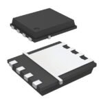 BSC106N025S G

The activity of extra discounts on wholesale prices is in full swing…
Please fill in your contact information and we will send you the latest wholesale price list.





