ChipApex | Global Electronic Components Supplier
SEARCH
Search Product
Search Post
— IC芯片 | 连接器 | 传感器 | 被动器件 —
Search productSearch post
— IC芯片 | 连接器 | 传感器 | 被动器件 —
Consult the customer manager about the wholesale price.
consultation hotline:86-132-6715-2157
email:[email protected]
Contact the product manager for consultation. One-stop consultation is available.
Do you want a lower wholesale price? Please send us your inquiry and we will reply immediately.
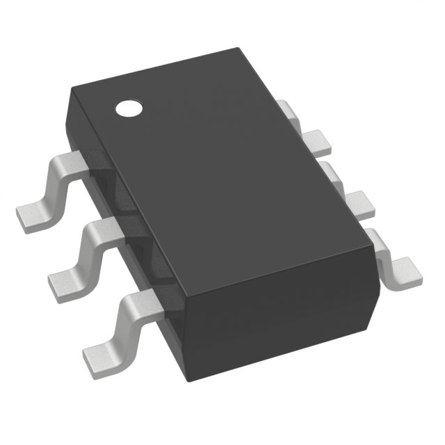
The BSL308PEH6327XTSA1 is a dual P-channel enhancement-mode MOSFET array from the OptiMOS™ P3 series, housed in a PG-TSOP-6 surface-mount package. It features a maximum drain-source voltage of -30 V and a continuous drain current of -2.0 A at 25 °C. The device has a typical gate charge of -5 nC and a maximum on-state resistance of 80 mΩ at VGS = -10 V. It operates within a temperature range of -55 °C to 150 °C and includes monolithic ESD protection rated for HBM Class 2.
Verify the complete part number against official Infineon documentation to ensure correct suffix alignment. Confirm that the specific ordering code matches the required tape and reel packaging format. Cross-reference the datasheet revision to validate all electrical parameters before finalizing procurement specifications.
Select this component when a compact dual P-channel solution is required for low-power switching tasks. The TSOP-6 package provides a small footprint ideal for space-constrained designs. Ensure the application voltage remains below the -30 V rating and consider thermal derating for ambient temperatures exceeding 25 °C.
This component belongs to the OptiMOS™ P3 family of small-signal transistors designed by Infineon Technologies. The series focuses on optimizing the trade-off between on-resistance and gate charge for efficient power management in compact electronic devices.
BSL308PE
The maximum pulsed drain current is -8.0 A at an ambient temperature of 25 °C.
Yes, the single-pulse avalanche energy rating is -10.7 mJ when driven at -2 A with a gate resistance of 25 Ω.
The reverse recovery time is typically 14 ns, and the reverse recovery charge is approximately -5.9 nC under specified test conditions.
 BSL308PEH6327XTSA1
The activity of extra discounts on wholesale prices is in full swing…
Please fill in your contact information and we will send you the latest wholesale price list.