ChipApex | Global Electronic Components Supplier

SEARCH
Search Product
Search Post
— IC芯片 | 连接器 | 传感器 | 被动器件 —
Search productSearch post
— IC芯片 | 连接器 | 传感器 | 被动器件 —
Consult the customer manager about the wholesale price.
consultation hotline:86-132-6715-2157
email:[email protected]
Contact the product manager for consultation. One-stop consultation is available.
Do you want a lower wholesale price? Please send us your inquiry and we will reply immediately.
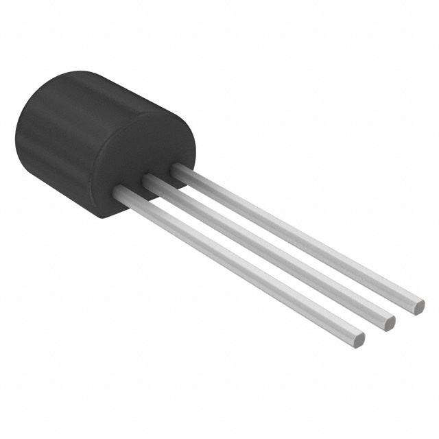
BSN254,126 is listed in the Single FETs, MOSFETs range at ChipApex. The manufacturer field lists NXP USA Inc.. Its product description is MOSFET N-CH 250V 310MA TO92-3. Review the specifications below when checking this part for your BOM.
The BSN254,126 is an N-channel enhancement mode vertical D-MOS transistor manufactured by NXP USA Inc. It operates within a SOT54 (TO-92) variant package and supports a maximum drain-source voltage of 250 V and a continuous drain current of 310 mA. The device features a low on-state resistance of 5 Ω at 300 mA and includes direct interface compatibility with C-MOS and TTL logic. Thermal performance is defined by a junction-to-ambient thermal resistance of 125 K/W.
Verify the specific ordering suffix against the manufacturer's latest documentation to confirm pinning variants and packaging details. Ensure that application conditions remain within the absolute maximum ratings provided in the datasheet to prevent permanent damage. Confirm compliance with relevant environmental directives such as RoHS before finalizing procurement specifications.
Select this component when high-voltage isolation up to 250 V is required in a compact through-hole package. Evaluate the thermal resistance characteristics against the expected power dissipation levels in the target circuit design. Consider the transfer admittance and capacitance values for high-frequency switching applications requiring fast response times.
This device belongs to the discrete semiconductor category, specifically functioning as an N-channel enhancement mode vertical D-MOS transistor. It is designed for general-purpose switching applications where robust voltage handling and reliable operation are necessary. The product specification supersedes earlier data from June 1997.
Consult the official datasheet for available pinning variants. Verify functional equivalence regarding voltage ratings and package dimensions before substituting with other N-channel MOSFETs.
The maximum DC drain-source voltage is 250 V.
Yes, it allows direct interface to C-MOS and TTL logic families.
Explore related parts through FETs, MOSFETs, Transistors, Discrete Semiconductor Products, all product categories.
 BSN254,126

The activity of extra discounts on wholesale prices is in full swing…
Please fill in your contact information and we will send you the latest wholesale price list.