 ChipApex | Global Electronic Components Supplier
SEARCH
Search Product
Search Post
— IC芯片 | 连接器 | 传感器 | 被动器件 —
Search productSearch post
— IC芯片 | 连接器 | 传感器 | 被动器件 —
Consult the customer manager about the wholesale price.
consultation hotline:86-132-6715-2157
email:[email protected]
Contact the product manager for consultation. One-stop consultation is available.
Do you want a lower wholesale price? Please send us your inquiry and we will reply immediately.
The BSO150N03MDGXUMA1 is a dual N-channel OptiMOS™ 3 M-Series Power-MOSFET in a PG-DSO-8 package. It features a maximum drain-source voltage of 30 V and continuous drain current of 9.3 A at 25 °C. The device exhibits low on-resistance, with a maximum R DS(on) of 15 mΩ at V GS=10 V and 18.2 mΩ at V GS=4.5 V. Gate charge is typically 6.1 nC at 4.5 V and 12.6 nC at 10 V. Thermal resistance from junction to soldering point is 50 K/W. Operating temperature ranges from -55 °C to 150 °C.
Verify the component against the official Infineon datasheet revision 1.1 to confirm electrical parameters and package marking. Ensure the ordering suffix matches the required reel quantity specifications. Confirm RoHS compliance and halogen-free status according to IEC61249-2-21 standards before integration into consumer-grade designs.
Select this component for designs requiring dual channels in a compact surface-mount footprint. The logic-level gate drive capability supports efficient operation with 4.5 V control signals. Evaluate thermal management requirements based on the specified junction-to-soldering point resistance for steady-state and pulsed operations.
This part belongs to the OptiMOS™ 3 M-Series, designed specifically for consumer electronics applications. It utilizes silicon technology within a PG-DSO-8 plastic package. The series emphasizes low on-resistance and fast switching characteristics suitable for modern portable device power architectures.
Check pinout compatibility and thermal resistance values when substituting. Verify that alternative dual N-channel MOSFETs meet the 30 V breakdown and 9.3 A current requirements. Ensure gate threshold voltage ranges align with the 5V driver system constraints.
The maximum pulsed drain current is 65 A at an ambient temperature of 25 °C.
No, the datasheet specifies that the BSO150N03MD G is qualified for consumer level applications only.
The typical reverse transfer capacitance (Crss) is 2 pF at V DS=15 V and f=1 MHz.
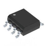 BSO150N03MDGXUMA1
The activity of extra discounts on wholesale prices is in full swing…
Please fill in your contact information and we will send you the latest wholesale price list.





