 ChipApex | Global Electronic Components Supplier
SEARCH
Search Product
Search Post
— IC芯片 | 连接器 | 传感器 | 被动器件 —
Search productSearch post
— IC芯片 | 连接器 | 传感器 | 被动器件 —
Consult the customer manager about the wholesale price.
consultation hotline:86-132-6715-2157
email:[email protected]
Contact the product manager for consultation. One-stop consultation is available.
Do you want a lower wholesale price? Please send us your inquiry and we will reply immediately.
The BSO203P is a P-Channel OptiMOS-P small-signal transistor in an SO-8 package. It features a drain-source voltage of -20 V and a continuous drain current of -8.2 A at 25°C. The device exhibits a maximum on-state resistance of 21 mΩ at VGS=-4.5 V. It supports Super Logic Level operation rated for 2.5 V gate drive. The component is avalanche rated with single-pulse energy up to 97 mJ and dv/dt rated at -6 kV/µs. Operating temperature ranges from -55°C to +150°C.
Verify the specific ordering code Q67042-S4072 matches the required SO-8 package variant. Confirm that the preliminary data status does not impact long-term availability or final specification stability for your production timeline. Ensure thermal management designs account for the specified junction-to-soldering point thermal resistance values under actual PCB footprint conditions.
Select this component when a P-Channel MOSFET with low gate threshold voltage is required for logic-level interfacing. The -20 V rating suits low-voltage DC systems. Consider the 21 mΩ RDS(on) for conduction loss calculations at high currents. Verify that the SO-8 package thermal dissipation capabilities meet the system's power requirements without excessive heatsinking.
This part belongs to Infineon's OptiMOS-P family, designed for small-signal power switching. The technology emphasizes low on-resistance and fast switching speeds within a compact surface-mount package. It targets applications requiring efficient control of moderate current loads in consumer and industrial electronics where space and cost are critical constraints.
No public confirmed substitute part numbers are documented in the provided datasheet. Cross-referencing requires independent verification of pinout, electrical ratings, and package dimensions against potential alternatives.
The absolute maximum gate-source voltage is ±12 V.
Yes, the BSO203P is avalanche rated with a single pulse avalanche energy of 97 mJ under specified test conditions.
The reverse recovery time (trr) is typically 35.7 ns and maximally 44.6 ns under standard test conditions.
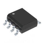 BSO203PNTMA1
The activity of extra discounts on wholesale prices is in full swing…
Please fill in your contact information and we will send you the latest wholesale price list.





