 ChipApex | Global Electronic Components Supplier

SEARCH
Search Product
Search Post
— IC芯片 | 连接器 | 传感器 | 被动器件 —
Search productSearch post
— IC芯片 | 连接器 | 传感器 | 被动器件 —
Consult the customer manager about the wholesale price.
consultation hotline:86-132-6715-2157
email:[email protected]
Contact the product manager for consultation. One-stop consultation is available.
Do you want a lower wholesale price? Please send us your inquiry and we will reply immediately.
BSP295H6327XTSA1 is listed in the Single FETs, MOSFETs range at ChipApex. The manufacturer field lists Infineon Technologies. Its product description is MOSFET N-CH 60V 1.8A SOT223-4. Review the specifications below when checking this part for your BOM.
The BSP295H6327XTSA1 is an N-channel enhancement-mode MOSFET from Infineon's SIPMOS series, housed in a PG-SOT223 surface-mount package. It features a maximum drain-source voltage of 60 V and a continuous drain current of 1.8 A at 25°C. The device exhibits a typical on-state resistance of 0.3 Ω and a total gate charge of 14 nC. It supports a reverse diode with a forward voltage of 0.84 V and a dv/dt rating of 6 kV/µs. Qualified to AEC-Q101 standards, it operates within a temperature range of -55°C to +150°C.
Verify the specific ordering suffix H6327XTSA1 against official Infineon documentation to confirm tape and reel packaging quantities and marking details. Ensure compatibility with RoHS and halogen-free compliance requirements as stated in the datasheet. Cross-reference the component marking code BSP295 with the physical device to prevent counterfeit substitution during assembly.
Select this component when a 60 V N-channel MOSFET with low gate charge is required for automotive or industrial environments. Consider the thermal resistance values and safe operating area curves for heat dissipation planning. Evaluate the reverse diode specifications if synchronous rectification or freewheeling functions are needed in the circuit design.
This part belongs to Infineon's SIPMOS small-signal transistor family, designed for compact surface-mount applications. The PG-SOT223 package provides a balance between power handling and board space efficiency. The BSP295 variant specifically targets low-voltage, medium-current switching tasks within the broader portfolio of automotive-grade silicon MOSFETs.
Consult official Infineon replacement guides for verified substitutes. Do not assume pin-compatible alternatives without verifying electrical parameters such as RDS(on) and breakdown voltage against the original specification sheet.
The maximum rated dv/dt is 6 kV/µs under conditions of IS=1.8A, VDS=40V, and di/dt=200A/µs.
The gate threshold voltage typically decreases as junction temperature increases, ranging from approximately 1.8 V at low temperatures to lower values at elevated temperatures.
The typical total gate charge is 14 nC when measured at VDD=24V, ID=1.8A, and VGS ranging from 0 to 10V.
Explore related parts through FETs, MOSFETs, Transistors, Discrete Semiconductor Products, all product categories.
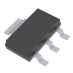 BSP295H6327XTSA1

The activity of extra discounts on wholesale prices is in full swing…
Please fill in your contact information and we will send you the latest wholesale price list.





