ChipApex | Global Electronic Components Supplier

SEARCH
Search Product
Search Post
— IC芯片 | 连接器 | 传感器 | 被动器件 —
Search productSearch post
— IC芯片 | 连接器 | 传感器 | 被动器件 —
Consult the customer manager about the wholesale price.
consultation hotline:86-132-6715-2157
email:[email protected]
Contact the product manager for consultation. One-stop consultation is available.
Do you want a lower wholesale price? Please send us your inquiry and we will reply immediately.
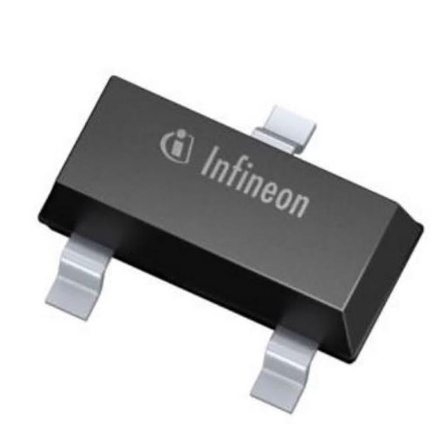
The BSS139IXTSA1 is an N-channel depletion mode small-signal transistor manufactured by Infineon Technologies. It operates within a drain-source voltage range of up to 250 V and supports a continuous drain current of 0.1 A at 25 °C. The device features a maximum on-state resistance of 30 Ω at zero gate bias, with a typical value of 12.5 Ω. It utilizes the PG-SOT23-3 surface-mount package and is qualified for industrial applications according to JEDEC standards.
Verify the specific ordering suffix XTSA1 against official Infineon documentation to confirm tape-and-reel packaging specifications. Ensure that the component meets all relevant environmental compliance requirements, including RoHS and halogen-free standards, before finalizing procurement decisions for production integration.
Select this component when high-voltage handling and depletion mode functionality are required in a compact SMD form factor. Consider the thermal resistance characteristics and power dissipation limits relative to the intended operating temperature range. Evaluate the on-state resistance values to ensure compatibility with low-current switching requirements.
This part belongs to the BSS139I series of small-signal transistors designed for robust performance in demanding environments. The series emphasizes reliability through strict adherence to industrial testing protocols. It serves as a specialized solution for applications requiring precise control over N-channel depletion behavior.
Consult official Infineon cross-reference guides for verified substitutes. Do not assume functional equivalence based solely on package or voltage ratings without verifying electrical parameters.
The gate threshold voltage ranges from -2.1 V to -1 V under specified test conditions.
Dynamic characteristics such as turn-on delay and rise time are provided in the datasheet for evaluating high-frequency performance.
 BSS139IXTSA1

The activity of extra discounts on wholesale prices is in full swing…
Please fill in your contact information and we will send you the latest wholesale price list.